
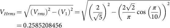
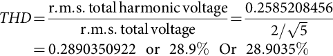
Hence, total harmonic distortion is
15.4.1.3 Pulse Width Modulation Mode of Operation
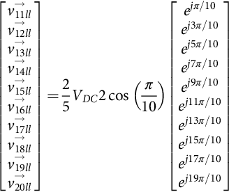
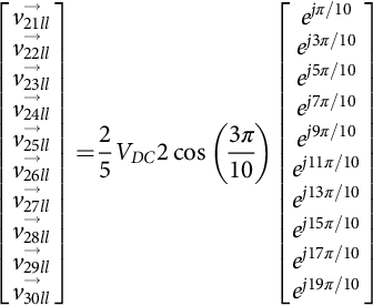
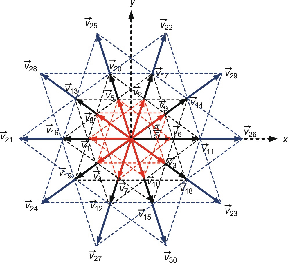
If a five-phase voltage-source inverter is operated in PWM mode, apart from the already described 10 states, there are additional 22 switching states. These remaining 22 switching states encompass three possible situations: all the states when four switches from upper (or lower) half and one from the lower (or upper) half of the inverter are on (states 11–20), two states when either all the five upper (or lower) switches are “on” (states 31 and 32), and the remaining states with three switches from the upper (lower) half and two switches from the lower (upper) half in conduction mode (states 21–30). The corresponding space vectors for 11–30 are obtained using Eq. (15.68), and it is seen that the total of 32 space vectors, available in the PWM operation, fall into four distinct categories regarding the magnitude of the available output phase voltages. The phase voltage space vectors are summarized in Table 15.4 for all 32 switching states and are shown in Fig. 15.32.

Table 15.4
Phase-to-neutral voltage space vectors for states 1–32
| Space vectors | Value of the space vectors |
| v1phase to v10phase | |
| v11phase to v20phase | |
| v21phase to v30phase | |
| v31phase to v32phase | 0 |
Since adjacent line voltage yields lower output value, only nonadjacent line voltages are elaborated as well:
15.4.1.4 Model Transformation Using Decoupling Matrix
Since the system under discussion is a five-phase one, the complete model can be only be elaborated in five-dimensional space. The first two-dimensional spaces are d-q, the second one is named as x-y, and the last is zero-sequence components that are absent due to the assumption of isolated neutral. On the basis of the general decoupling transformation matrix for an n-phase system, inverter voltage space vectors in the second two-dimensional subspace (x-y) are determined with Eq. (15.92):
Thus, 32 space vectors of phase-to-neutral voltage in the x-y plane are obtained using Eq. (15.92) and are demonstrated in Fig. 15.33.
It can be seen from Figs. 15.32 and 15.33 that the outer decagon space vectors of the ![]() plane map into the innermost decagon of the x-y plane, the innermost decagon of d-q plane forms the outer decagon of x-y plane while the middle decagon space vector map into the same region. Further, it is observed from the above mapping that the phase sequence a,b,c,d,e of
plane map into the innermost decagon of the x-y plane, the innermost decagon of d-q plane forms the outer decagon of x-y plane while the middle decagon space vector map into the same region. Further, it is observed from the above mapping that the phase sequence a,b,c,d,e of ![]() plane corresponds to a,c,e,b,d in x-y that are basically the third harmonic voltages.
plane corresponds to a,c,e,b,d in x-y that are basically the third harmonic voltages.
15.4.1.5 Hardware Implementation of a Five-Phase VSI in 180 Conduction Mode
Hardware can be developed to implement the square-wave operation of a five-phase voltage-source inverter. The hardware can be developed using available power switch modules from different manufacturers such as Semikron, Mitsubishi, and Fairchild. The power switches are available in discrete form to implement inverter system. The gate driver circuit is also available from different manufacturers. The control can be implemented using microcontroller, digital signal processors (DSP), dSpace, and field-programmable gate arrays (FPGA). The control codes can be written in C/C++. Some of the DSPs and FPGAs are compatible with Matlab/Simulink, and hence, control codes can be implemented directly. In FPGA, system generator is used for writing the control code. System generator is a library in Matlab/Simulink software. The coding is done in the form of drag and drop in system generator.
15.4.1.6 Hardware Set-up
The control of inverter can be implemented using sophisticated controllers such as microcontroller, digital signal processors (DSP), dSpace, and field-programmable gate arrays (FPGA). The output voltages from these controllers are generally 3.3 V that is not enough for turning on the IGBTs/MOSFETs/BJT. Further to turn off the power switching devices, the gate capacitors are to be fully and rapidly discharged. Gate drive circuit is thus required to match the voltage level requirement of turning on the power switches (about 15 V), and a discharge path for the gate capacitor is needed. Hence, a gate drive circuit is needed to successfully turn on and turn off the power devices. The following section describes the implementation of the control, gate drive, and power circuit using analog devices. The complete block diagram is shown in Fig. 15.34.
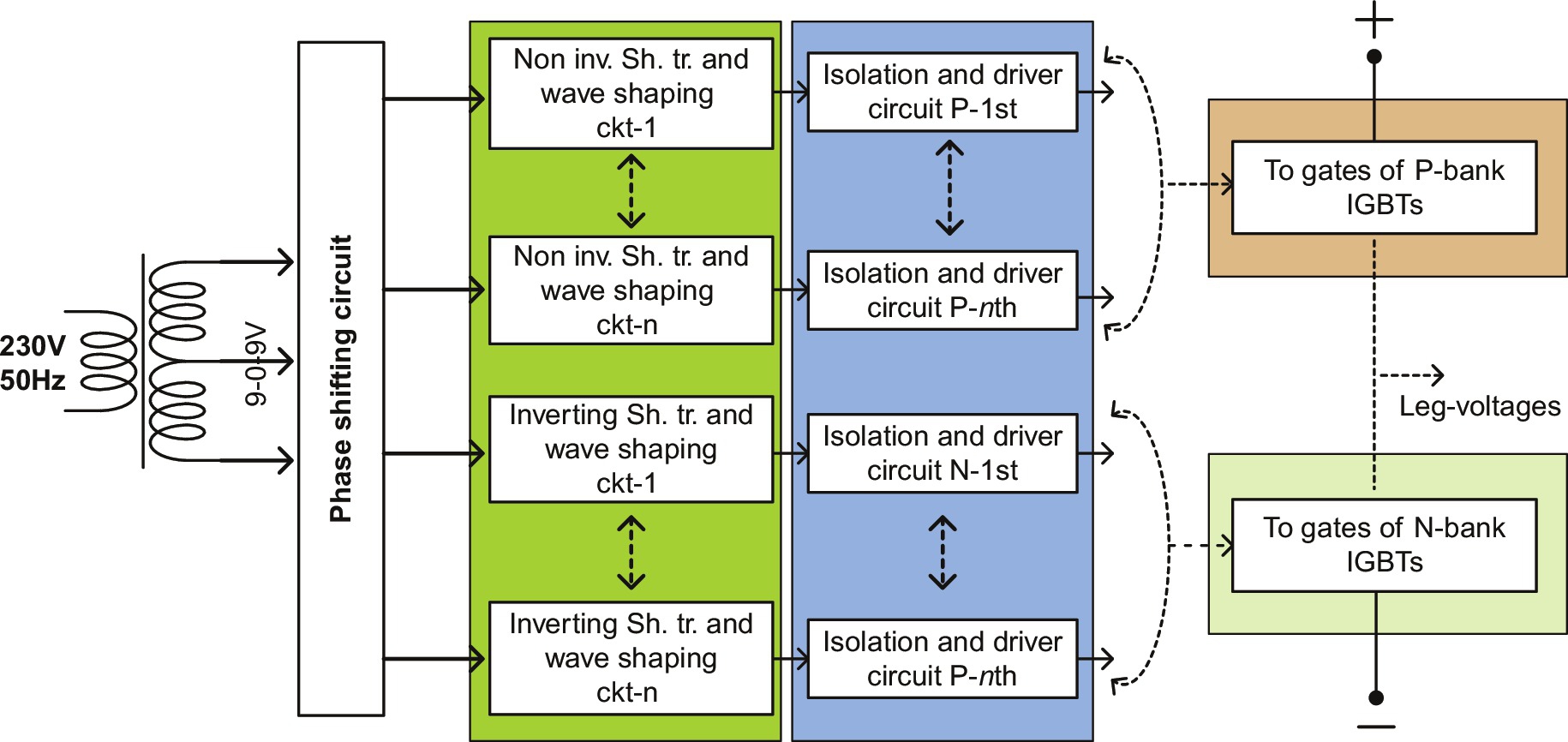
Power supply is obtained from a single-phase grid and is converted to 9-0-9 V using a transformer. The converted voltage of (9-0-9 V) is fed to the phase-shifting circuit shown in Fig. 15.35, to provide appropriate phase shift for operation at various conduction angle (the conduction angle refers to the conduction modes of inverter, e.g., 180, 144, and 108 degrees). The phase-shifted signal is then fed to the inverting/noninverting Schmitt trigger circuit and wave-shaping circuit (Figs. 15.36 and 15.37). The processed signal is then fed to the isolation and driver circuit shown in Fig. 15.38. This is then finally given to the gate of IGBTs. There are two separate circuits for upper and lower legs of the inverter.


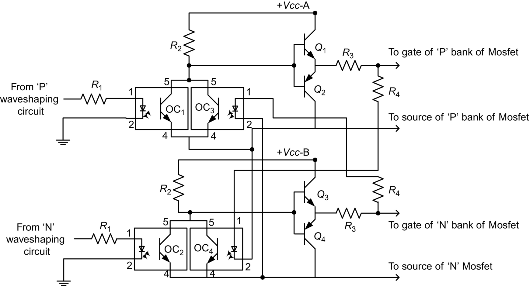
The power circuit is made up of IGBT SGW20N60 having a rating of 20 A and 600 V DC, with snubber circuit consisting of the series combination of a resistance and a capacitor with a diode in parallel with the resistance.
15.4.1.7 Hardware Results
Experiment can be conducted for stepped operation of inverter with 180 degrees conduction modes for star-connected five-phase resistive load. A single-phase supply can be given to the control circuit through the phase-shifting network. The output of the phase-shifting circuit provides the required five-phase output voltage by appropriately tuning it. These five-phase signals are then further processed to generate the gate drive circuit.
15.4.1.8 Results of 180 Degrees Conduction Mode
The output from the Schmitt trigger circuit is presented in Fig. 15.39. The driving control gate/base signals for the 10-step mode for legs A–B of the inverter are illustrated in Fig. 15.40. The corresponding phase voltage thus obtained is shown in Fig. 15.41, keeping the DC-link voltage at 60 V. The output phase voltage is called 10 step in one fundamental cycle (1/5Vdc, 2/5Vdc, 1/5Vdc, 2/5Vdc, 1/5Vdc, −1/5Vdc, −2/5Vdc, −1/5Vdc, −2/5Vdc, and −1/5Vdc).

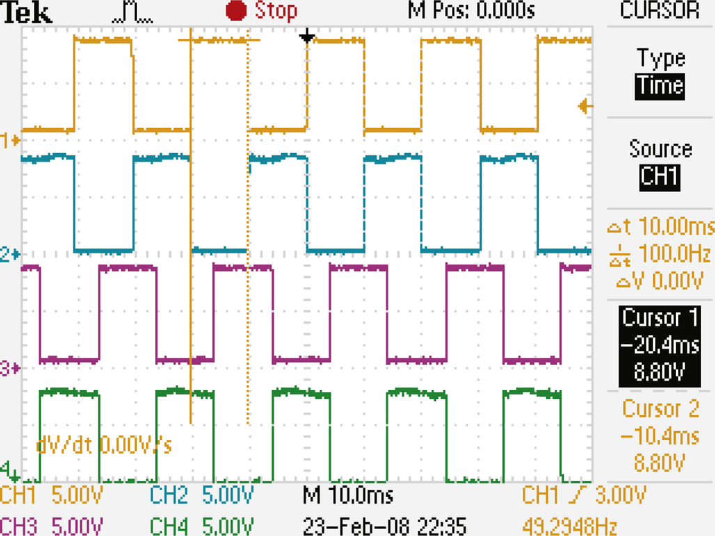
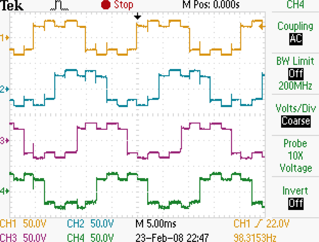
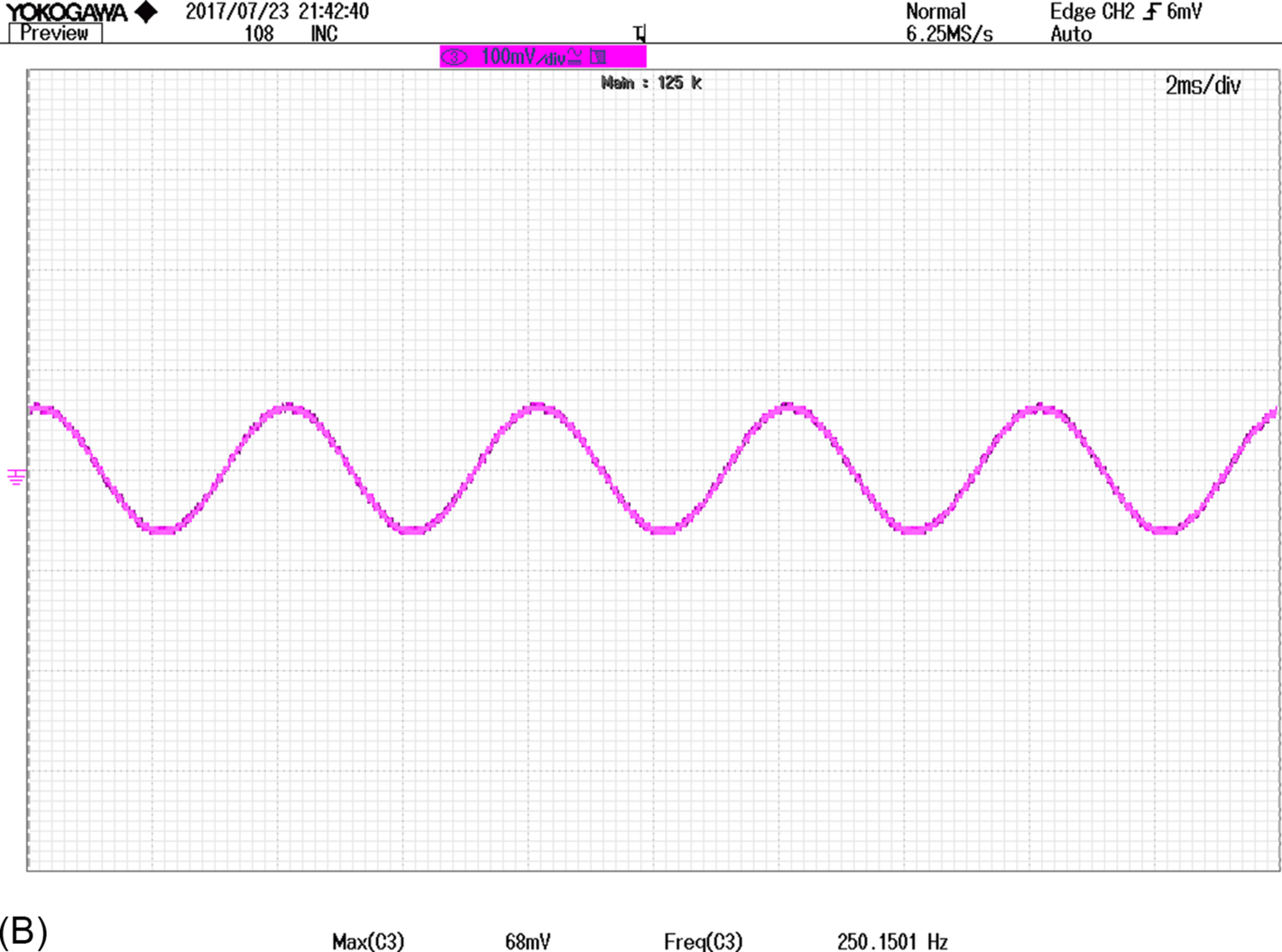
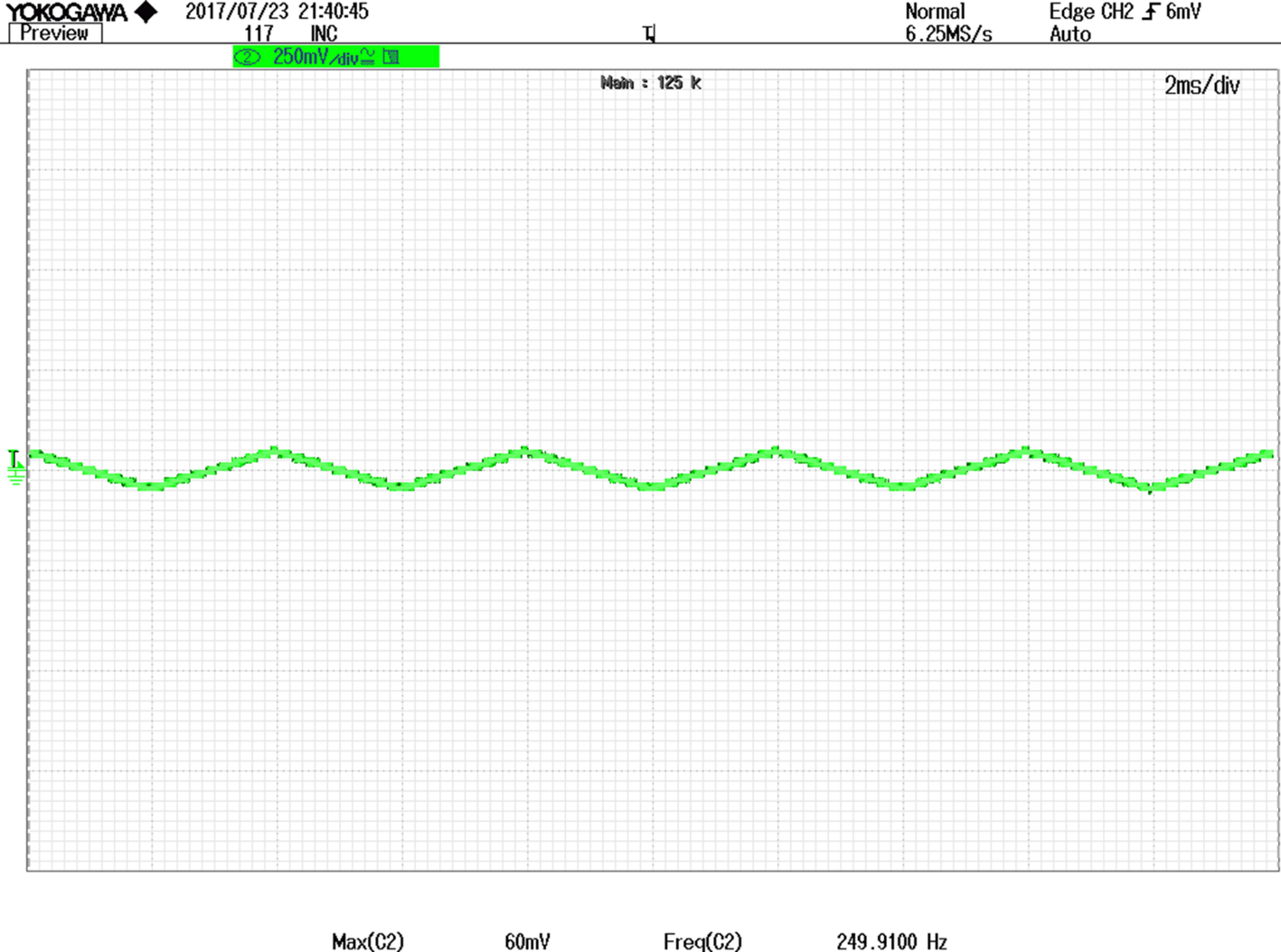
Nonadjacent line voltage obtained is shown in Fig. 15.42. All currents are measured using AC/DC current probe giving the output of 100 mV/A.

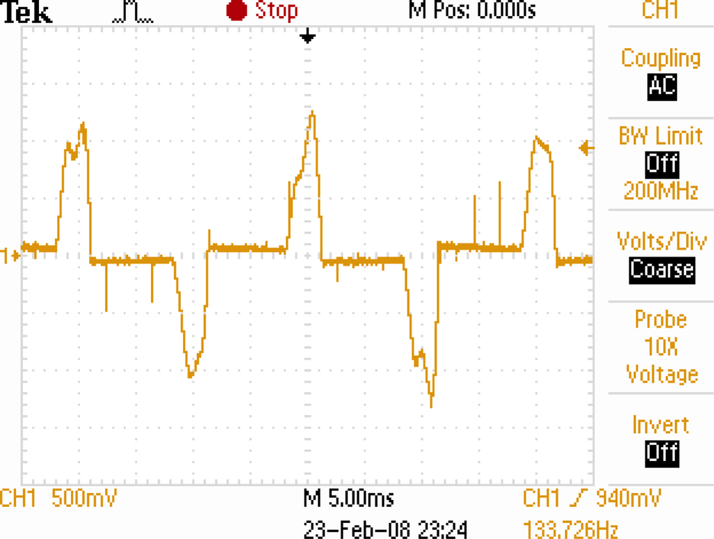
The AC side input current is also measured and is depicted in Fig. 15.43. The analysis is presented in the last subsection.
15.4.1.9 DSP Implementation of Step Mode of Operation
The results obtained in Section 15.4.1.9 are verified using implementation through TMS320F2812 DSP under the same operating conditions. Control code is written in C++ and run in PC. It is transferred to the DSP using serial communication cable RS232. The DSP generate 10 gating signals that are fed to the power module of the inverter. The detail experimental setup is provided in Section 15.4.1.10. All the three conduction angles are implemented. The developed algorithm is verified using a star-connected resistive load and a five-phase induction machine.
15.4.1.10 180 Degrees Conduction Mode
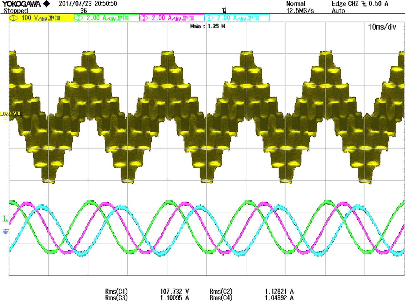
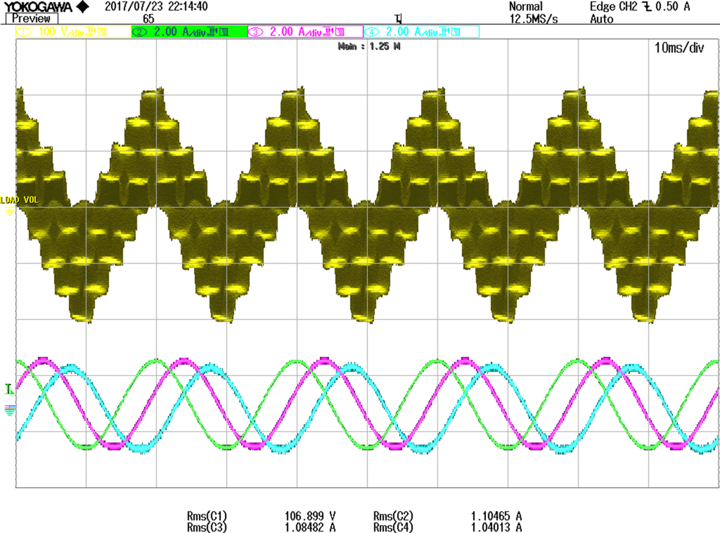
The inverter is operated in 180 degrees conduction mode, and a five-phase star-connected resistive load is connected across the output terminal. The resulting phase voltage, nonadjacent line voltages are illustrated in Figs. 15.44 and 15.45, respectively.
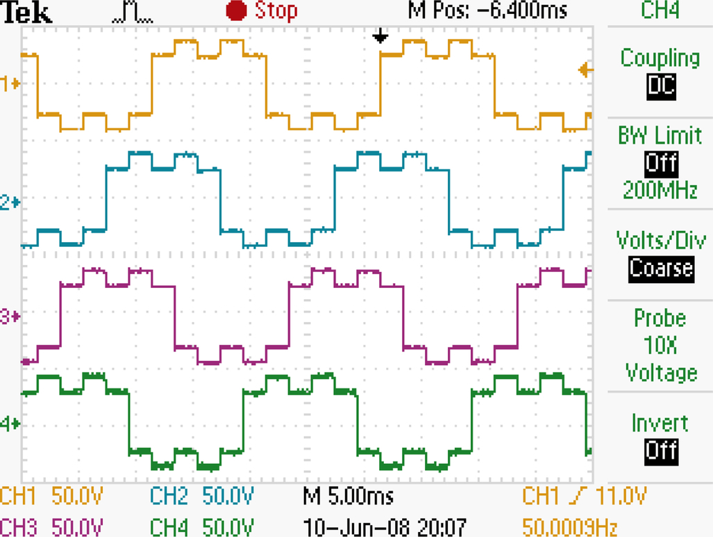
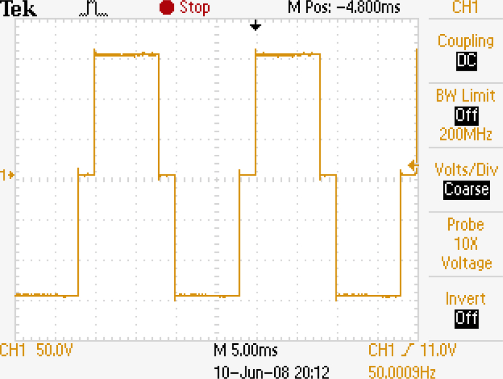
It is observed that the phase voltage generated using cheap analog-circuit-based inverter shown in Fig. 15.41 is identical to the one obtained using DSP as shown in Fig. 15.44. Similarly, the nonadjacent line voltage of Fig. 15.42 is identical to the one shown in Fig. 15.45. This verifies the correct design of the analog-based inverter and also verifies the DSP code. The same study is carried out using a five-phase induction motor as a load. The resulting voltage and stator current waveforms are presented in Fig. 15.46. The waveform is typical for such load.

15.4.2 Carrier-Based PWM
15.4.2.1 With Zero Sequence Signal
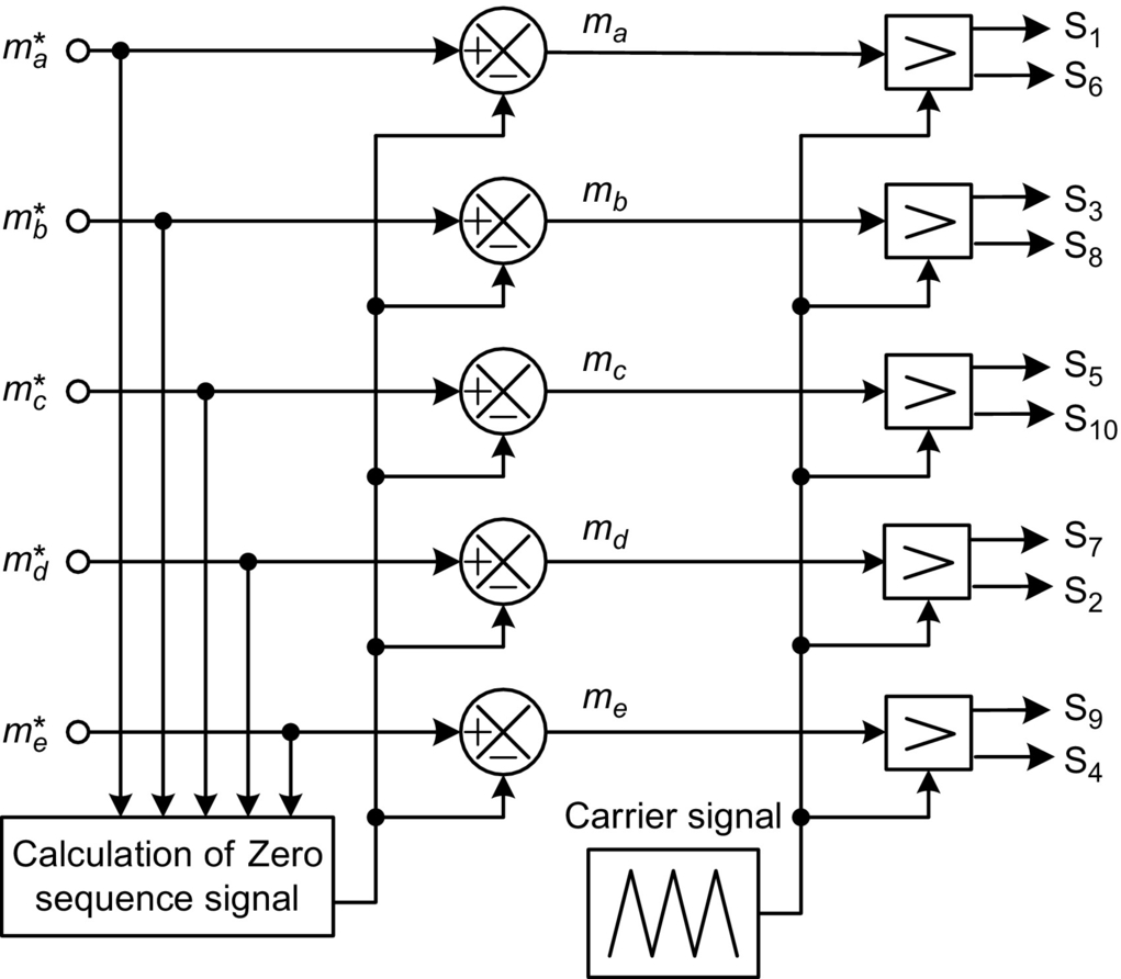
Carrier-based sinusoidal PWM is the most popular and widely used PWM technique because of their simple implementation in both analog and digital realization [32,34]. The principle of carrier-based PWM true for a three-phase VSI is also applicable to a multiphase VSI. The PWM signal is generated by comparing a sinusoidal modulating signal with a triangular (double edge) or a saw-tooth (single edge) carrier signal. The frequency of the carrier is normally kept much higher compared to the modulating signal. The principle of operation of a carrier-based PWM modulator is shown in Fig. 15.47, and generation of PWM waveform is illustrated in Fig. 15.48. Modulation signals are obtained using five fundamental sinusoidal signals (displaced in time by ![]() ), which are summed with an appropriate zero-sequence signal. These modulation signals are compared with high-frequency carrier signal (saw-tooth or triangular shape), and all five switching functions for inverter legs are obtained directly. In general, modulation signal can be expressed as
), which are summed with an appropriate zero-sequence signal. These modulation signals are compared with high-frequency carrier signal (saw-tooth or triangular shape), and all five switching functions for inverter legs are obtained directly. In general, modulation signal can be expressed as
where ![]() and vnN represents zero-sequence signal and vi⁎ is fundamental sinusoidal signals. Zero-sequence signal represents a degree of freedom that exits in the structure of a carrier-based modulator, and it is used to modify modulation signal waveforms and thus to obtain different modulation schemes. Continuous PWM schemes are characterized by the presence of switching activity in each of the inverter legs over the carrier signal period, as long as peak value of the modulation signal does not exceed the carrier magnitude.
and vnN represents zero-sequence signal and vi⁎ is fundamental sinusoidal signals. Zero-sequence signal represents a degree of freedom that exits in the structure of a carrier-based modulator, and it is used to modify modulation signal waveforms and thus to obtain different modulation schemes. Continuous PWM schemes are characterized by the presence of switching activity in each of the inverter legs over the carrier signal period, as long as peak value of the modulation signal does not exceed the carrier magnitude.
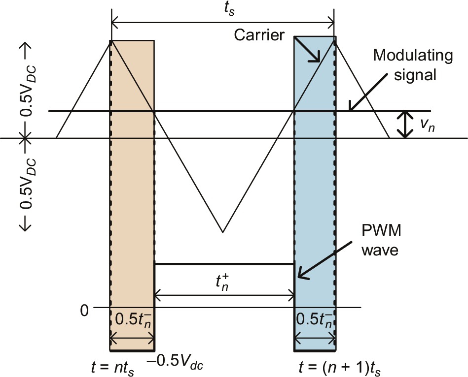
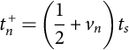
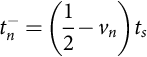
The following relationship holds true in Fig. 15.48:
where
where ![]() and
and ![]() are the positive and negative pulse widths in the nth sampling interval, respectively, and vn is the normalized amplitude of modulation signal. The normalization is done with respect to Vdc. Eqs. (15.95) and (15.96) are referred as the equal volt-second principle as applied to a three-phase inverter [32,35,36]. The normalized peak value of the triangular carrier wave is
are the positive and negative pulse widths in the nth sampling interval, respectively, and vn is the normalized amplitude of modulation signal. The normalization is done with respect to Vdc. Eqs. (15.95) and (15.96) are referred as the equal volt-second principle as applied to a three-phase inverter [32,35,36]. The normalized peak value of the triangular carrier wave is ![]() in linear region of operation. Modulator gain has the unity value while operating in the linear region, and peak value of inverter output fundamental voltage is equal to the peak value of the fundamental sinusoidal signal. Thus, the maximum output phase voltages from a five-phase VSI are limited to 0.5 p.u. This is also evident in [32,37]. Thus, the output phase voltage from a three-phase and a five-phase VSI are the same when utilizing carrier-based PWM.
in linear region of operation. Modulator gain has the unity value while operating in the linear region, and peak value of inverter output fundamental voltage is equal to the peak value of the fundamental sinusoidal signal. Thus, the maximum output phase voltages from a five-phase VSI are limited to 0.5 p.u. This is also evident in [32,37]. Thus, the output phase voltage from a three-phase and a five-phase VSI are the same when utilizing carrier-based PWM.
15.4.2.2 Sinusoidal Pulse Width Modulation (SPWM)
The simplest continuous carrier-based PWM is obtained with the selection of the zero-sequence signal as ![]() . Modulation signals for all five inverter legs are equal to five sinusoidal fundamental signals. Thus, while operating in the linear region, maximum value of the modulation index of the SPWM has the unity value,
. Modulation signals for all five inverter legs are equal to five sinusoidal fundamental signals. Thus, while operating in the linear region, maximum value of the modulation index of the SPWM has the unity value, ![]() . Modulation index is defined as the ratio of the fundamental component amplitude of the line-to-neutral inverter output voltage to one-half of the available DC bus voltage. Thus,
. Modulation index is defined as the ratio of the fundamental component amplitude of the line-to-neutral inverter output voltage to one-half of the available DC bus voltage. Thus,

where V1 is the fundamental output phase voltage.
15.4.2.3 Fifth Harmonic Injection PWM
The effect of the addition of harmonic with reverse polarity in any signal is to reduce the peak of the reference signal. Aim here is to bring the amplitude of the reference as low as possible, so that the reference can then be pushed to make it equal to the carrier, resulting in the higher output voltage and better DC bus utilization. Using this principle, third harmonic injection PWM scheme is used in a three-phase VSI that results in increase in the fundamental output voltage to 0.575Vdc [32,35]. Third harmonic voltages do not appear in the output phase voltages and are restricted to the leg voltages only. Following the same principle, fifth harmonic injection PWM scheme can be developed to increase the modulation index of a five-phase VSI.
The reference leg voltages are given as

It is to be noted that fifth harmonic has no effect on the value of the reference waveform when ![]() , since
, since ![]() for all odd k. Thus, M5 is chosen to make the peak magnitude of the reference of (15.98) that occurs where the fifth harmonic is zero. This ensures the maximum possible value of the fundamental component. The reference voltage reaches a maximum when
for all odd k. Thus, M5 is chosen to make the peak magnitude of the reference of (15.98) that occurs where the fifth harmonic is zero. This ensures the maximum possible value of the fundamental component. The reference voltage reaches a maximum when
This yield

Thus, the maximum modulation index can be determined from
The above equation gives

Thus, the output fundamental voltage is increased by 5.15% higher than the value obtainable using simple carrier-based PWM by injecting 6.18% fifth harmonic in fundamental. The fifth harmonic is in opposite phase to that of the fundamental.
15.4.2.4 Offset or Triangular Zero-Sequence Injection PWM
Another way of increasing the modulation index is to add an offset voltage to the references. This will effectively do the same function as above. The offset voltage is given as
where ![]() and
and ![]() . Note that this is the same as for a three-phase inverter.
. Note that this is the same as for a three-phase inverter.
In case of three-phase VSI, the offset voltage is simply third harmonic triangular wave of 25% magnitude of fundamental. The peak of the fundamental is 0.575 p.u., (0.406 p.u. rms), the peak of the resultant modulating signal is 0.5 p.u. (0.353 p.u. rms), and the peak of the offset is 0.147 p.u. (0.104 p.u. rms). Hence, offset peak is 25% of the fundamental peak.
In a five-phase VSI, the offset is found as the fifth-harmonic triangular wave of 9.55% of the fundamental input reference. This value has been established by simulations. Offset addition requires only addition operation and hence is suitable for practical implementation.
A generalized formula of offset voltage is obtained, which is to be injected along with the fundamental in case of five-phase VSI. The expression is
where Vmax is the maximum of the five-phase references, Vmin is the minimum of the five-phase references, and μ is the factor that decides the placement of the two zero-vector states. If it is 0.5, then the two zero states are placed equally, and this corresponds to symmetrical zero-vector placement.
It is important to note that not only the fifth harmonic but also all the additional 5k (k=1,3,5…) harmonics are included in the modulation signal in this technique. Maximum modulation index has the same value as in the previous case, ![]() . To illustrate the effects of fifth-harmonic and triangular signal injection, the overall modulating signals are shown in Fig. 15.49.
. To illustrate the effects of fifth-harmonic and triangular signal injection, the overall modulating signals are shown in Fig. 15.49.
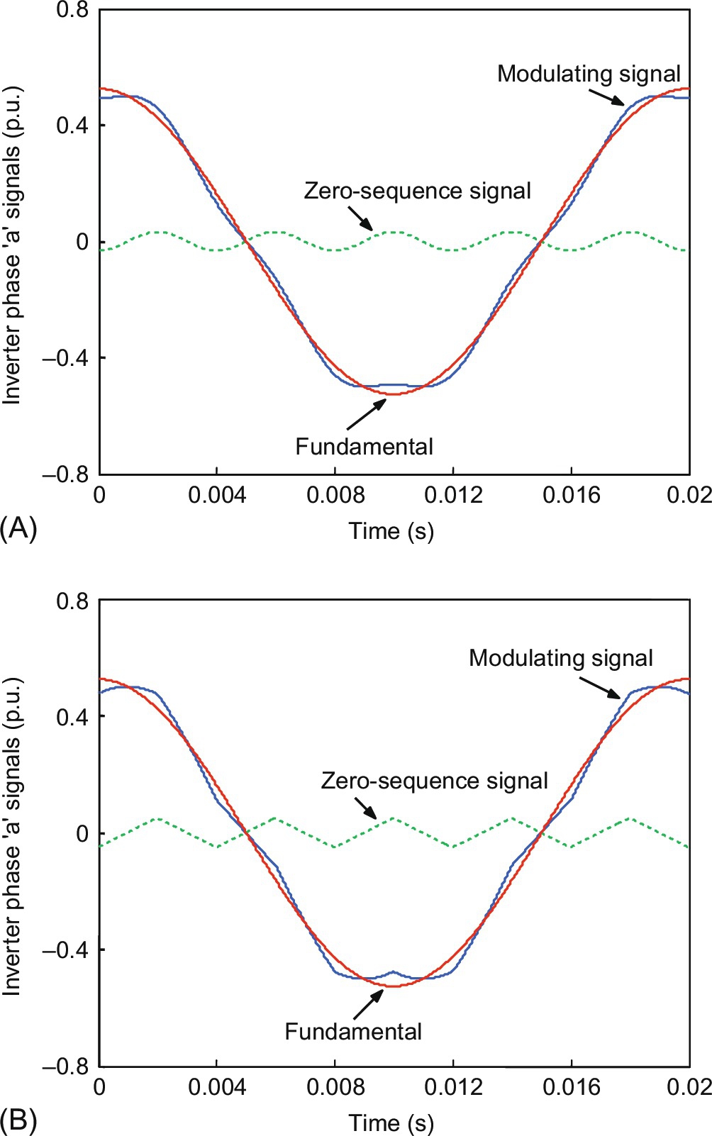
In general, an extension of the linear region is obtained through the repositioning of the peak value of the modulating signal. While sinusoidal fundamental signals have peak values at ![]() , zero sequence modifies this, and now, peak values of the modulating signals occur at
, zero sequence modifies this, and now, peak values of the modulating signals occur at ![]() Hence, for five-phase carrier-based continuous PWM methods with zero-sequence signal addition, new peak values of modulating signals appear at angles
Hence, for five-phase carrier-based continuous PWM methods with zero-sequence signal addition, new peak values of modulating signals appear at angles ![]() . This allows the peak value of the fundamental signal to exceed unity, up to the value when peak of the modulating signal reaches saturation level (
. This allows the peak value of the fundamental signal to exceed unity, up to the value when peak of the modulating signal reaches saturation level (![]() , in accordance with (15.97)). It is obvious from Fig. 15.49 that fifth-harmonic injection and offset injection have the same maximum value of the modulation index in the limit of the linear region.
, in accordance with (15.97)). It is obvious from Fig. 15.49 that fifth-harmonic injection and offset injection have the same maximum value of the modulation index in the limit of the linear region.
15.4.2.5 Space Vector Pulse Width Modulation
Space-vector pulse-width modulation has become one of the most popular PWM techniques because of its easier digital implementation and higher DC bus utilization, when compared with the sinusoidal PWM method. The principle of SVPWM lies in the switching of inverter in a special way to apply a set of space vector for specific time. There is a lot of flexibility available in choosing the proper space-vector combination for an effective control of multiphase VSIs because of the large numbers of space vectors available in multiphase power converters.
Advantages of space vector PWM:
i. SVPWM increases fundamental output without distorting line-to-line waveform.
ii. The fundamental output of SVPWM is 94.02% that is 15.47% greater than sinusoidal PWM of 78.55% fundamental.
iii. SVPWM compares a single modulating wave with a carrier instead of using three waves.
iv. When the neutral of the load is connected to a DC supply voltage, SVPWM considers interaction among phases, whereas other PWM method does not.
v. Designing of heat sinks is an important factor for power dissipation. Power dissipation includes conduction and switching loss. Switching losses in sine PWM is difficult to compute that depend on modulation index, while computation is easier in space-vector PWM.
vi. SVPWM implementation is completely digital.
vii. Vector control implementation is completely digital, and thus, it is easy to implement SVPWM-based vector control scheme.
viii. Over modulation can easily be implemented.
ix. For high modulation index, the harmonics of current and torque of space-vector PWM will be much less than sine PWM.
In the case of a five-phase VSI, there are a total of 25=32 space vectors available, of which 30 are active state vectors and two are zero state vectors forming three concentric decagons. For the implementation of space-vector PWM in linear range, two different approaches can be adopted. One approach is the simple extension of method used in a three-phase inverter (use of two adjacent large length vectors) and second approach where four adjacent vectors are used (two large and two medium lengths). The first approach gives higher output voltage; however, the output voltages contain lower-order harmonics, more specifically, the third and seventh. The second approach offers sinusoidal output voltage; however, the magnitude is lower.
The first approach used only 10 outer large length vectors to implement the symmetrical SVPWM. Two neighboring active space vectors and two zero space vectors are utilized in one switching period to synthesize the input reference voltage. In total, 20 switchings take place in one switching period, so that the state of each switch is changed twice. The switching is done in such a way that, in the first switching half period, the first zero vector is applied, followed by two active state vectors and then by the second zero state vector. The second switching half period is the mirror image of the first one. The symmetrical SVPWM is achieved in this way. This method is the simplest extension of space-vector modulation of three-phase VSIs.
An ideal SVPWM of a five-phase inverter should satisfy a number of requirements. Firstly, in order to keep the switching frequency constant, each switch can change state only twice in the switching period (once “on” to “off” and once “off” to “on” or vice versa). Secondly, the rms value of the fundamental phase voltage of the output must be equal to the rms of the reference space vector. Thirdly, the scheme must provide full utilization of the available DC bus voltage. Finally, since the inverter is aimed at supplying the load with sinusoidal voltages, the low-order harmonic content needs to be minimized (this especially applies to the third and seventh harmonic). These criteria are used in assessing the merits and demerits of various SVPWM.
15.4.2.6 Space Vector PWM for Sinusoidal Output
The purpose here is to generate sinusoidal output phase voltages using space-vector PWM. Application of two neighboring medium active space vectors together with two large active space vectors in each switching period makes it possible to maintain zero average value in the second plane and consequently providing sinusoidal output. Use of four active space vectors per switching period requires the calculation of four application times, labeled here tal,tbl,tam,tbm. The expressions used for the calculation of dwell times of various space vector are [32,38]
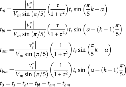
where ![]() . This is in essence allocates 61.8% more dwell times to large space vectors compared with medium space vector, thus satisfying the constraints of producing zero average voltage in the x-y plane. This can be more clearly seen from Fig. 15.50.
. This is in essence allocates 61.8% more dwell times to large space vectors compared with medium space vector, thus satisfying the constraints of producing zero average voltage in the x-y plane. This can be more clearly seen from Fig. 15.50.

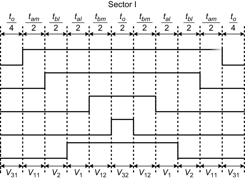
It is seen from Fig. 15.50 that the vectors in x-y plane are in such a position to cancel each other by using the dwell time Eq. (15.104). The applications of active and zero space vectors are arranged in such a way as to obtain a symmetrical SVPWM. The space-vector disposition in sector I is illustrated in Fig. 15.51. Modulation signals of SVPWM are identical to those obtained with offset addition. Switching pattern is a symmetrical PWM with two commutations per inverter leg. The space vectors are applied in odd sectors using sequence ![]() , while the sequence is
, while the sequence is ![]() in even sectors.
in even sectors.
It can be easily observed from Eq. (15.104) that the zero-vector application time remains positive for ![]() . Thus, the output phase voltage from a VSI using this Space Vector PWM scheme is 0.5257Vdc, which is 5.15% higher compared with the output obtainable with carrier-based sinusoidal PWM without harmonic injection and equal to the output obtainable with zero-sequence (fifth-harmonic) signal injection.
. Thus, the output phase voltage from a VSI using this Space Vector PWM scheme is 0.5257Vdc, which is 5.15% higher compared with the output obtainable with carrier-based sinusoidal PWM without harmonic injection and equal to the output obtainable with zero-sequence (fifth-harmonic) signal injection.
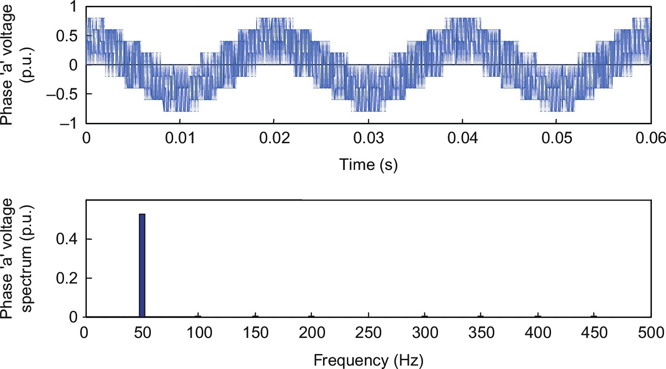
Simulation is carried out using Matlab/Simulink to implement the SVPWM with application of four active and a zero vector. The resulting waveform and harmonic spectrum are shown in Fig. 15.52. The average leg voltage is depicted in Fig. 15.51, and it is observed that the leg voltage is now quite similar to one obtained in three-phase VSI. The phase voltage is completely sinusoidal without any low-order harmonics. The spectrum of phase voltage shows the maximum achievable output equals to 0.5257 p.u. (keeping DC-link voltage equals to unity).
15.4.2.7 Experimental Implementation
Experimental setup is prepared in the laboratory to implement the carrier-based and space-vector PWM techniques discussed in the previous section. A five-phase voltage-source inverter is developed using intelligent power module. Texas Instrument DSP TMS320F2812 is used as the processor to implement the control algorithm. Since this DSP can be coded in C or C++, it is more user-friendly, and they have dedicated 16 hardware PINS to generate the desired PWM signals. The PWM circuits associated with compare units make it possible to generate up to eight PWM output channels (per Event Manger) with programmable dead band and polarity. This DSP is specifically meant for use in motor drive purposes, and it can control up to eight-phase two-level inverter. The control code is written in C++ language in Code composer studio 3.1 that runs in a PC. The control signal generated by PC is transferred to the DSP board through RS 232 cable connected in parallel printer port of the PC. The DSP board is connected to the power module through dedicated control cable. The DSP interfacing circuit along with required A/D and D/A converter is built on the DSP board itself procured from VI Microsystems.
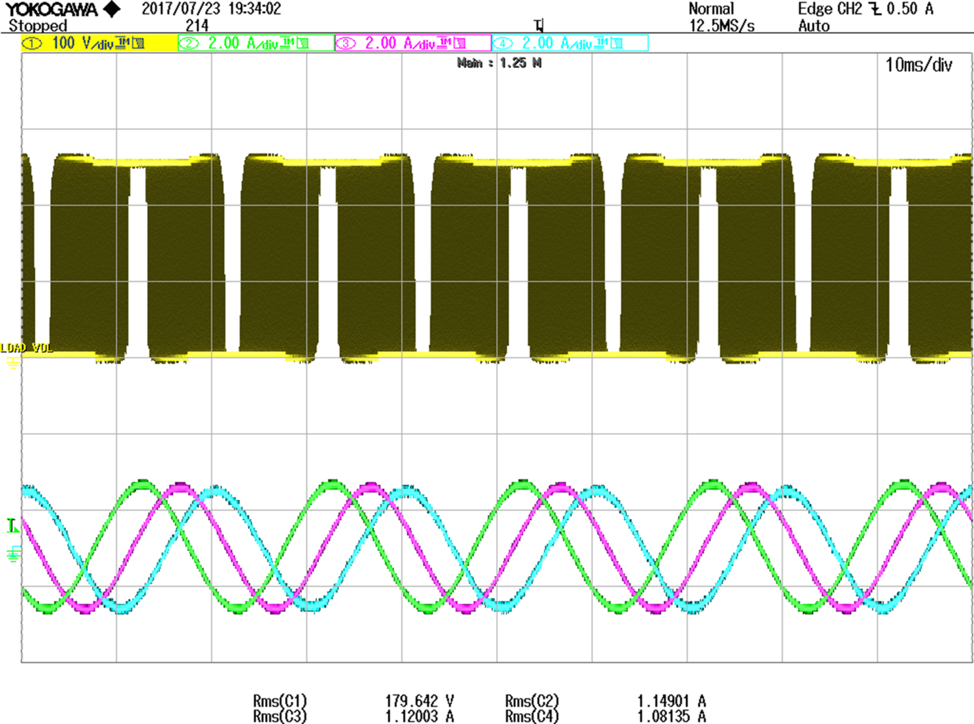
Five-phase carrier-based PWM is implemented keeping the switching frequency equal to 10 kHz. The resulting waveform of leg voltage and corresponding phase voltage along with phase ‘a', ‘b', and ‘c' are shown in Figs. 15.53 and 15.54, respectively.

Fifth-harmonic injection scheme is also implemented using DSP coding with fifth-harmonic signal equal to 0.0618 p.u. The resulting waveform of leg and corresponding phase voltage (unfiltered) are shown in Figs. 15.55 and 15.56, respectively.

Triangular zero sequence injection PWM (TIPWM) is also implemented. The resulting waveform of phase voltage along with phase ‘a', ‘b', and ‘c' currents and triangular zero-sequence injection are shown in Figs. 15.57 and 15.58, respectively.
15.4.3 Modeling and Control of a Seven-Phase VSI-Square Wave Mode
This section details the modeling and control of a seven-phase VSI. The modeling of seven-phase VSI is done for 14-step operation using space-vector approach [39]. The PWM operation mode is elaborated in Section 15.4.4 [40,41]. Conventional 180 degrees conduction mode is considered. The procedure adopted here follows from Section 15.4.1. The analytic expressions for harmonic components and THD are derived for phase voltages and second nonadjacent line voltages. The same is then verified using simulation and experimental results.
Section 15.4.3.2 deals with the modeling and control of a seven-phase voltage-source inverter in pulse-width modulation mode. There are a total of 128 switching state where the first 14 states lead to 14-step mode of operation and the rest of 114 switching states fall in PWM mode. Out of total 128 space vectors, two space vectors corresponding to the switching states 0000000 and 1111111 yield null vectors, and the rest 126 that produce finite length vectors are called active vectors. The model obtained is transformed into three different planes, namely, d-q, x1-y1, and x2-y2. Out of these three planes, only d-q produces torque in the machines supplied by the inverter, while the space vectors of other planes produce distortion in the stator currents. The complete model using space-vector approach is elaborated. The simulation results are included to validate the modeling procedure.
15.4.3.1 Fourteen-Step Operation of a Seven-Phase Voltage Source Inverter
Power circuit topology of a seven-phase VSI is shown in Fig. 15.59. Each switch in the circuit consists of two power semiconductor devices, connected in antiparallel. One of these is a fully controllable semiconductor, such as a bipolar transistor or IGBT, while the second one is a diode. The input of the inverter is a DC voltage, which is regarded further on as being constant. The inverter outputs are denoted in Fig. 15.59 with lowercase symbols (a,b,c,d,e,f,g), while the points of connection of the outputs to inverter legs have symbols in capital letters (A,B,C,D,E,F,G). The basic operating principles of the seven-phase VSI are developed in what follows assuming the ideal commutation and zero forward voltage drops. Each switch is assumed to conduct for 180 degrees, leading to the operation in the 14-step mode. Phase delay between firing of two switches in any subsequent two phases is equal to 360/7 degrees=51.43 degrees (approx.).
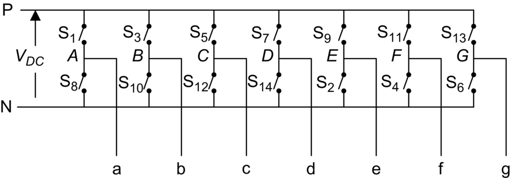
The driving control gate/base signals for the 14 switches of the inverter in Fig. 15.59 are illustrated in Fig. 15.60. One complete cycle of operation of the inverter can be divided into 14 distinct modes indicated in Fig. 15.60 and summarized in Table 15.5. It follows from Fig. 15.60 and Table 15.5 that at any instant of time there are seven switches that are “on” and seven switches that are “off.” In the 14-step mode of operation, there are three conducting switches from the upper 7 and 4 from the lower 7 or vice versa.

Table 15.5
Fourteen-step operation of a seven-phase VSI
| States | Switches ON | Terminal polarity |
| 12 | 1,9,10,11,12,13,14 | A+ B− C− D− E+ F+ G+ |
| 13 | 10,11,12,13,14,12 | A+ B− C− D− E− F+ G+ |
| 14 | 11,12,13,14,1,2,3 | A+ B+ C− D− E− F+ G+ |
| 1 | 12,13,14,1,2,3,4 | A+ B+ C− D− E− F− G+ |
| 2 | 13,14,1,2,3,4,5 | A+ B+ C+ D− E− F− G+ |
| 3 | 14,1,2,3,4,5,6 | A+ B+ C+ D− E− F− G− |
| 4 | 1,2,3,4,5,6,7 | A+ B+ C+ D+ E− F− G− |
| 5 | 2,3,4,5,6,7,8 | A− B+ C+ D+ E− F− G− |
| 6 | 3,4,5,6,7,8,9 | A− B+ C+ D+ E+ F− G− |
| 7 | 4,5,6,7,8,9,10 | A− B− C+ D+ E+ F− G− |
| 8 | 5,6,7,8,9,10,11 | A− B− C+ D+ E+ F+ G− |
| 9 | 6,7,8,9,10,11,12 | A− B− C− D+ E+ F+ G− |
| 10 | 7,8,9,10,11,12,13 | A− B− C− D+ E+ F+ G+ |
| 11 | 8,9,10,11,12,13,14 | A− B− C− D− E+ F+ G+ |
Leg voltages (i.e., voltages between points A,B,C,D,E,F,G and the negative rail of the DC bus N in Fig. 15.59) are considered first. The leg voltages obtained from the gate drive signal of Fig. 15.60.
Space-vector model of the inverter is developed in the following subsection. Space vector of phase voltages in stationary reference frame is defined, using power invariant transformation, as
where a=exp(j2π/7), a2=exp(j4π/7), ![]() , a⁎=exp(−j2π/5),
, a⁎=exp(−j2π/5), ![]() ,
, ![]() , and ⁎ stands for a complex conjugate.
, and ⁎ stands for a complex conjugate.
Space vectors of leg voltages are obtained using Fig. 15.60 and Eq. (15.105) and are given as in Eq. (15.106).

It is seen that the leg voltages have magnitude of (2/7)VDC(2 cos (π/7)) and are 25.7142857 degrees spatially apart.
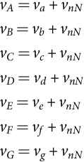
Phase-to-neutral voltages of the star-connected load are most easily found by defining a voltage difference between the star point n of the load and the negative rail of the DC bus N. The following correlation then holds true:
Since the phase voltages in a star-connected load sum to zero, the summation of Eq. (15.107) yields
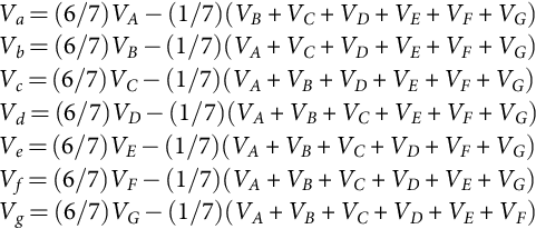
Substitution of (15.107) into (15.108) yields phase-to-neutral voltages of the load in the following form:
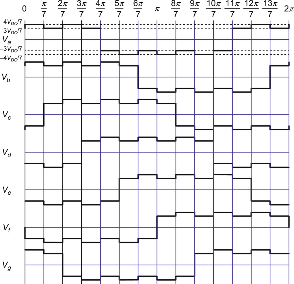
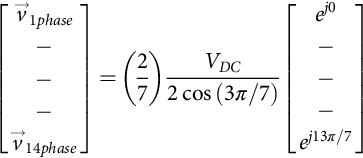
The phase voltages in different modes are obtained by substituting leg voltages into Eq. (15.109), and their space vectors are determined using Eq. (15.105). The waveform of phase voltages for seven phases is shown in Fig. 15.61. The space vectors for the first 14 states are obtained as
The Fourier analysis can be carried out, recognizing the quarter-wave symmetry; the waveform may be considered as odd function. The Fourier coefficients are obtained as

The expression in third bracket of Eq. (15.111) equals to zero for all the harmonics whose order is divisible by seven. Hence, one can write the phase-to-neutral voltages as

From (15.112), it follows that the fundamental component of the output phase-to-neutral voltages has an rms value equal to
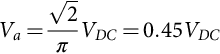
From Fig. 15.61, the mean square value is determined as


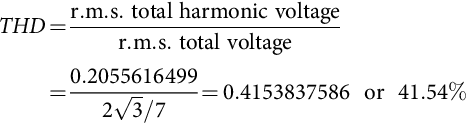
Total harmonic rms voltage (p.u.) is given by

Hence, total harmonic distortion is
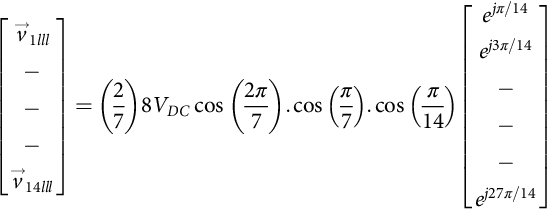
There are three systems of line-to-line voltage: adjacent, first nonadjacent and second nonadjacent, in contrast to a three-phase system where only one line-to-line voltage is defined and five-phase system where two systems of line voltages exist. The second nonadjacent line voltages yield highest magnitude, and hence, it is taken up for discussion, and the other two types are omitted. The values of line voltages are obtained as the difference between the leg voltages and are plotted in Fig. 15.62.

The second nonadjacent line-line voltage space vectors are calculated by substituting the values from Table 15.6 into the defining expression (15.105) and are
Table 15.6
Second nonadjacent line-to-line voltages of seven-phase VSI
| States | Switches ON | Space vectors | Vad | Vbe | Vcf | Vdg | Vea | Vfb | Vgc |
| 1 | 12,13,14,1,2,3,4 | VDC | VDC | 0 | -VDC | -VDC | -VDC | VDC | |
| 2 | 13,14,1,2,3,4,5 | VDC | VDC | VDC | -VDC | -VDC | -VDC | 0 | |
| 3 | 14,1,2,3,4,5,6 | VDC | VDC | VDC | 0 | -VDC | -VDC | VDC | |
| 4 | 1,2,3,4,5,6,7 | 0 | VDC | VDC | VDC | -VDC | -VDC | -VDC | |
| 5 | 2,3,4,5,6,7,8 | -VDC | VDC | VDC | VDC | 0 | -VDC | -VDC | |
| 6 | 3,4,5,6,7,8,9 | -VDC | 0 | VDC | VDC | VDC | -VDC | -VDC | |
| 7 | 4,5,6,7,8,9,10 | -VDC | -VDC | VDC | VDC | VDC | 0 | -VDC | |
| 8 | 5,6,7,8,9,10,11 | -VDC | -VDC | 0 | VDC | VDC | VDC | -VDC | |
| 9 | 6,7,8,9,10,11,12 | -VDC | -VDC | -VDC | VDC | VDC | VDC | 0 | |
| 10 | 7,8,9,10,11,12,13 | -VDC | -VDC | -VDC | 0 | VDC | VDC | VDC | |
| 11 | 8,9,10,11,12,13,14 | 0 | -VDC | -VDC | -VDC | VDC | VDC | VDC | |
| 12 | 1,9,10,11,12,13,14 | VDC | -VDC | -VDC | -VDC | 0 | VDC | VDC | |
| 13 | 10,11,12,13,14,12 | VDC | 0 | -VDC | -VDC | -VDC | VDC | VDC | |
| 14 | 11,12,13,14,1,2,3 | VDC | VDC | -VDC | -VDC | -VDC | 0 | VDC |

Fourier analysis can be done, and the resulting coefficients of the Fourier series for second nonadjacent line-to-line voltages, by considering odd quarter-wave symmetry, are
The series will be
From (15.120), it follows that the fundamental component of the output phase-to-neutral voltages has an rms value equal to
From Fig. 15.62, the mean square value is determined as

Total harmonic rms voltage (p.u.) is given by

Hence, total harmonic distortion is

The distortion in the line voltages is quite high.
It is important to note at this stage that the space vectors described by (15.105) provide mapping of inverter voltages into a two-dimensional space. However, since seven-phase inverter essentially requires description in a seven-dimensional space, not all the harmonics contained in (15.111) and (15.112) will be encompassed by the space vector of (15.105). In particular, space vectors calculated using (15.105) will only represent harmonics of the order 14k±1, k=0, 1,2,3….., that is, the 1st, the 13th, the 15th, and so on. Harmonics of the order 7k, k=1,2,3,…, cannot appear due to the isolated neutral point. However, harmonics of the order 7k±2 and 7k±4, k=1,3,5,… are present in (15.111) and (15.112) but are not encompassed by the space-vector definition of (15.105). These harmonics in essence appear in the second and third two-dimensional space, which requires introduction of the second and third space vectors for the seven-phase system. This issue is addressed in Section 15.4.3.3.
15.4.3.2 PWM Mode of Operation
If a seven-phase VSI is operated in PWM mode, apart from the already described 14 states, there will be additional 114 switching states. The number of possible switching states is in general equal to 2n, where n is the number of inverter legs (i.e., output phases). This correlation is valid for any two-level VSI. Table 15.7 summarizes the additional switching states that are associated with PWM mode of operation and are absent in the 14-step mode of operation. Switches that are “on” and the corresponding terminal polarity are included in Table 15.7 As can be seen from Table 15.7, the remaining 114 switching states encompass four possible situations: all the states when four switches from upper (or lower) half and three from the lower (or upper) half of the inverter are “on” (states 1–14, 29–42, 43–56, 85–99, and 98–112); two states when either all the seven upper (or lower) switches are “on” (states 127 and 128); all the states when five switches from upper (or lower) and two from upper (or lower) half of the inverter are “on” (states 15–28, 57–70, and 113–126); and remaining states with six switches from the upper (or lower) half and one switch from the lower (or upper) half in conduction mode (states 71–84). The phase-to-neutral voltages are described using the same approach as that of the previous sections.
Table 15.7
Modes of operation of seven-phase voltage-source inverter
| States | Switches ON | Polarity of terminal |
| 15 | 1,2,3,5,11,13,14 | A+B+C+D−E−F+G+ |
| 16 | 1,2,3,4,6,12,14 | A+B+C−D−E−F−G− |
| 17 | 1,2,3,4,5,7,13 | A+B+C+D+E−F−G+ |
| 18 | 2,3,4,5,6,8,14 | A−B+C+D−E−F−G− |
| 19 | 1,3,4,5,6,7,9 | A+B+C+D+E+F−G− |
| 20 | 2,4,5,6,7,8,10 | A−B−C+D+E−F−G− |
| 21 | 3,5,6,7,8,9,11 | A−B+C+D+E+F+G− |
| 22 | 4,6,7,8,9,10,12 | A−B−C−D+E+F−G− |
| 23 | 5,7,8,9,10,11,13 | A−B−C+D+E+F+G+ |
| 24 | 6,8,9,10,11,12,14 | A−B−C−D−E+F+G− |
| 25 | 7,9,10,11,12,13 | A+B−C−D+E+F+G+ |
| 26 | 2,8,10,11,12,13,14 | A−B−C−D−E−F+G+ |
| 27 | 1,3,9,11,12,13,14 | A+B+C−D−E+F+G+ |
| 28 | 1,2,4,10,12,13,14 | A+B−C−D−E−F−G+ |
| 29 | 1,2,4,5,10,13,14 | A+B−C+D−E−F+G+ |
| 30 | 1,2,3,5,6,11,14 | A+B+C+D−E−F+G− |
| 31 | 1,2,3,4,6,7,12 | A+B+C−D+E−F−G− |
| 32 | 2,3,4,5,7,8,13 | A−B+C+D+E−F−G+ |
| 33 | 3,4,5,6,8,9,14 | A−B+C+D−E+F−G− |
| 34 | 1,4,5,6,7,9,10 | A+B−C+D+E+F−G− |
| 35 | 2,5,6,7,8,10,11 | A−B−C+D+E−F+G− |
| 36 | 3,6,7,8,9,11,12 | A−B+C−D+E+F+G− |
| 37 | 4,7,8,9,10,12,13 | A−B−C−D+E+F−G+ |
| 38 | 5,8,9,10,11,13,14 | A−B−C+D−E+F+G+ |
| 39 | 1,6,9,10,11,12,14 | A+B−C−D−E+F+G− |
| 40 | 1,2,7,10,11,12,13 | A+B−C−D+E−F+G+ |
| 41 | 2,3,8,11,12,13,14 | A−B+C−D−E−F+G+ |
| 42 | 1,3,4,9,12,13,14 | A+B+C−D−E+F−G+ |
| 43 | 1,2,3,4,7,12,13 | A+B+C−D+E−F−G+ |
| 44 | 2,3,4,5,8,13,14 | A−B+C+D−E−F−G+ |
| 45 | 1,3,4,5,6,9,14 | A+B+C+D−E+F−G− |
| 46 | 1,2,4,5,6,7,10 | A+B−C+D+E−F−G− |
| 47 | 2,3,5,6,7,8,11 | A−B+C+D+E−F+G− |
| 48 | 3,4,6,7,8,9,12 | A−B+C−D+E+F−G− |
| 49 | 4,5,7,8,9,10,13 | A−B−C+D+E+F−G+ |
| 50 | 5,6,8,9,10,11,14 | A−B−C+D−E+F+G− |
| 51 | 1,6,7,9,10,11,12 | A+B−C−D+E+F+G− |
| 52 | 2,7,8,10,11,12,13 | A−B−C−D+E−F+G+ |
| 53 | 3,8,9,11,12,13,14 | A−B+C−D−E+F+G+ |
| 54 | 1,4,9,10,12,13,14 | A+B−C−D−E+F−G+ |
| 55 | 1,2,5,10,1,13,14 | A+B−C+D−E−F+G+ |
| 56 | 1,2,3,6,11,12,14 | A+B+C−D−E−F+G− |
| 57 | 2,3,4,8,12,13,14 | A−B+C−D−E−F−G+ |
| 58 | 1,3,4,5,9,13,14 | A+B+C+D−E+F−G+ |
| 59 | 1,2,4,5,6,10,14 | A+B−C+D−E−F−G− |
| 60 | 1,2,3,5,6,7,11 | A+B+C+D+E−F+G− |
| 61 | 2,3,4,6,7,8,12 | A−B+C−D+E−F−G− |
| 62 | 3,4,5,7,8,9,13 | A−B+C+D+E+F−G+ |
| 63 | 4,5,6,8,9,10,14 | A−B−C+D−E+F−G− |
| 64 | 1,5,6,7,9,10,11 | A−B−C+D+E+F+G− |
| 65 | 2,6,7,8,10,11,12 | A−B−C−D+E−F+G+ |
| 66 | 3,7,8,9,11,12,13 | A−B+C−D+E+F+G+ |
| 67 | 4,8,9,10,12,13,14 | A−B−C−D−E+F−G+ |
| 68 | 1,5,9,10,11,13,14 | A+B−C+D−E+F+G+ |
| 69 | 1,2,6,10,11,12,14 | A+B−C−D−E−F+G− |
| 70 | 1,2,3,7,11,12,13 | A+B+C−D+E−F+G+ |
| 71 | 1,2,4,6,10,12,14 | A+B−C−D−E−F−G− |
| 72 | 1,2,3,5,7,11,13 | A+B+C+D+E−F+G+ |
| 73 | 2,3,4,6,8,12,14 | A−B+C−D−E−F−G− |
| 74 | 1,3,4,5,7,9,13 | A+B+C+D+E+F−G+ |
| 75 | 2,4,5,6,8,10,14 | A−B−C+D−E−F−G− |
| 76 | 1,3,5,6,7,9,11 | A+B+C+D+E+F+G− |
| 77 | 2,4,6,7,8,10,12 | A−B−C−D+E−F−G− |
| 78 | 3,5,7,8,9,11,13 | A−B+C+D+E+F+G+ |
| 79 | 4,6,8,9,10,12,14 | A−B−C−D−E+F−G− |
| 80 | 1,5,7,9,10,11,13 | A+B−C+D+E+F+G+ |
| 81 | 2,6,8,10,11,12,14 | A−B−C−D−E−F+G− |
| 82 | 1,3,7,9,11,12,13 | A+B+C−D+E+F+G+ |
| 83 | 2,4,8,10,12,13,14 | A−B−C−D−E−F−G+ |
| 84 | 1,3,5,9,11,13,14 | A+B+C+D−E+F+G+ |
| 85 | 2,35,8,11,13,14 | A−B+C+D−E−F+G+ |
| 86 | 1,3,4,6,9,12,14 | A+B+C−D−E+F−G− |
| 87 | 1,2,4,5,7,10,13 | A+B−C+D+E−F−G+ |
| 88 | 2,3,5,6,8,11,14 | A−B+C+D−E−F+G− |
| 89 | 1,3,4,6,7,9,12 | A+B+C−D+E+F−G− |
| 90 | 2,4,5,7,8,10,13 | A−B−C+D+E−F−G+ |
| 91 | 3,5,6,8,9,11,14 | A−B+C+D−E+F+G− |
| 92 | 1,4,6,7,9,10,12 | A+B−C−D+E+F−G− |
| 93 | 2,5,7,8,10,11,13 | A−B−C+D+E−F+G+ |
| 94 | 3,6,8,9,11,12,14 | A−B+C−D−E+F+G− |
| 95 | 1,4,7,9,10,12,13 | A+B−C−D+E+F−G+ |
| 96 | 2,5,8,10,11,13,14 | A−B−C+D−E−F+G+ |
| 97 | 1,3,6,9,11,12,14 | A+B+C−D−E+F+G− |
| 98 | 1,2,4,7,10,12,13 | A+B−C−D+E−F−G+ |
| 99 | 1,2,5,6,10,11,14 | A+B−C+D−E−F+G− |
| 100 | 1,2,3,6,7,11,12 | A+B+C−D+E−F+G− |
| 101 | 2,3,4,7,8,12,13 | A−B+C−D+E−F−G+ |
| 102 | 3,4,5,8,9,13,14 | A−B+C+D−E+F−G+ |
| 103 | 1,4,5,6,9,10,14 | A+B−C+D−E+F−G− |
| 104 | 1,2,5,6,7,10,11 | A+B−C+D+E−F+G− |
| 105 | 2,3,6,7,8,11,12 | A−B+C−D+E−F+G− |
| 106 | 3,4,7,8,9,12,13 | A−B+C−D+E+F−G+ |
| 107 | 4,5,8,9,10,13,14 | A−B−C+D−E+F−G+ |
| 108 | 1,5,6,9,10,11,14 | A+B−C+D−E+F+G− |
| 109 | 1,2,6,7,10,11,12 | A+B−C−D+E−F+G− |
| 110 | 2,3,7,8,11,12,13 | A−B+C−D+E−F+G+ |
| 111 | 3,4,8,9,12,13,14 | A−B+C−D−E+F−G+ |
| 112 | 1,4,5,9,10,13,14 | A+B−C+D−E+F−G+ |
| 113 | 1,3,4,7,9,12,13 | A+B+C−D+E+F−G+ |
| 114 | 2,4,5,8,10,13,14 | A−B−C+D−E−F−G+ |
| 115 | 1,3,5,6,9,11,14 | A+B+C+D−E+F+G− |
| 116 | 1,2,4,6,7,10,12 | A+B−C−D+E−F−G− |
| 117 | 2,3,5,7,8,11,13 | A−B+C+D+E−F+G+ |
| 118 | 3,4,6,8,9,12,14 | A−B+C−D−E+F−G− |
| 119 | 1,4,5,7,9,10,13 | A+B−C+D+E+F−G+ |
| 120 | 2,5,6,8,10,11,14 | A−B−C+D−E−F+G− |
| 121 | 1,3,6,7,9,11,12 | A+B+C−D+E+F+G− |
| 122 | 2,4,7,8,10,12,13 | A−B−C−D+E−F−G+ |
| 123 | 3,5,8,9,11,13,14 | A−B+C+D−E+F+G+ |
| 124 | 1,4,6,9,10,12,14 | A+B−C−D−E+F−G− |
| 125 | 1,2,5,7,10,11,13 | A+B−C+D+E−F+G+ |
| 126 | 2,3,6,8,11,12,14 | A−B+C−D−E−F+G− |
| 127 | 2,4,6,8,10,12,14 | A−B−C−D−E−F−G− |
| 128 | 1,3,5,7,9,11,13 | A+B+C+D+E+F+G+ |
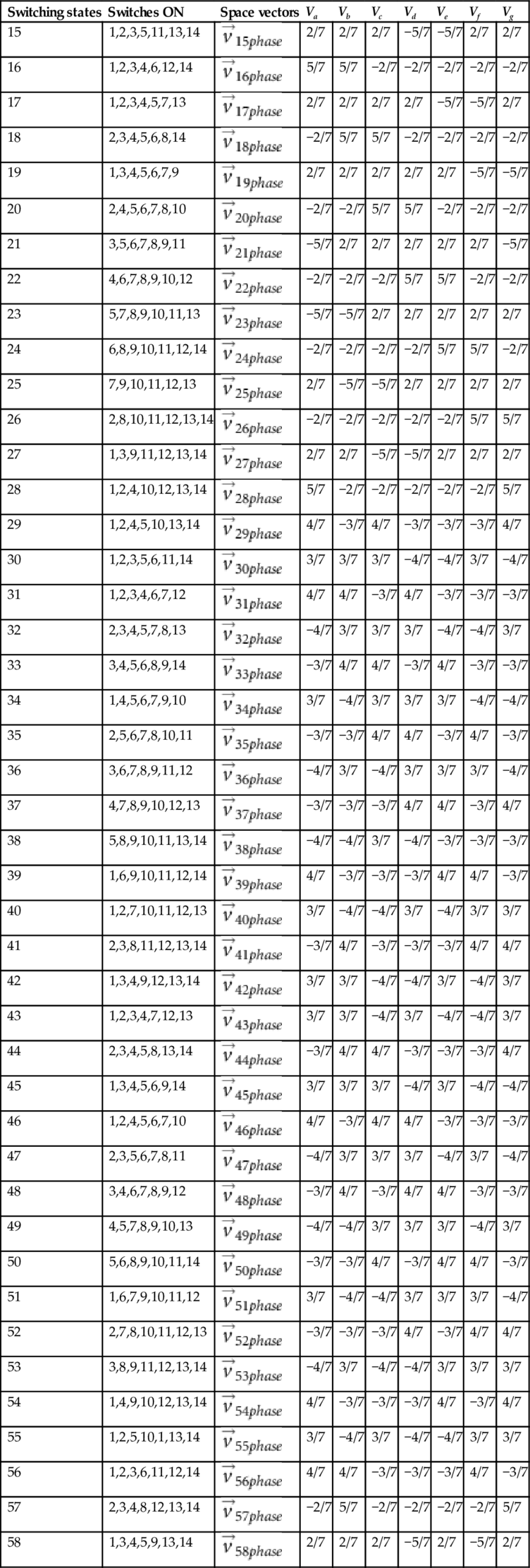
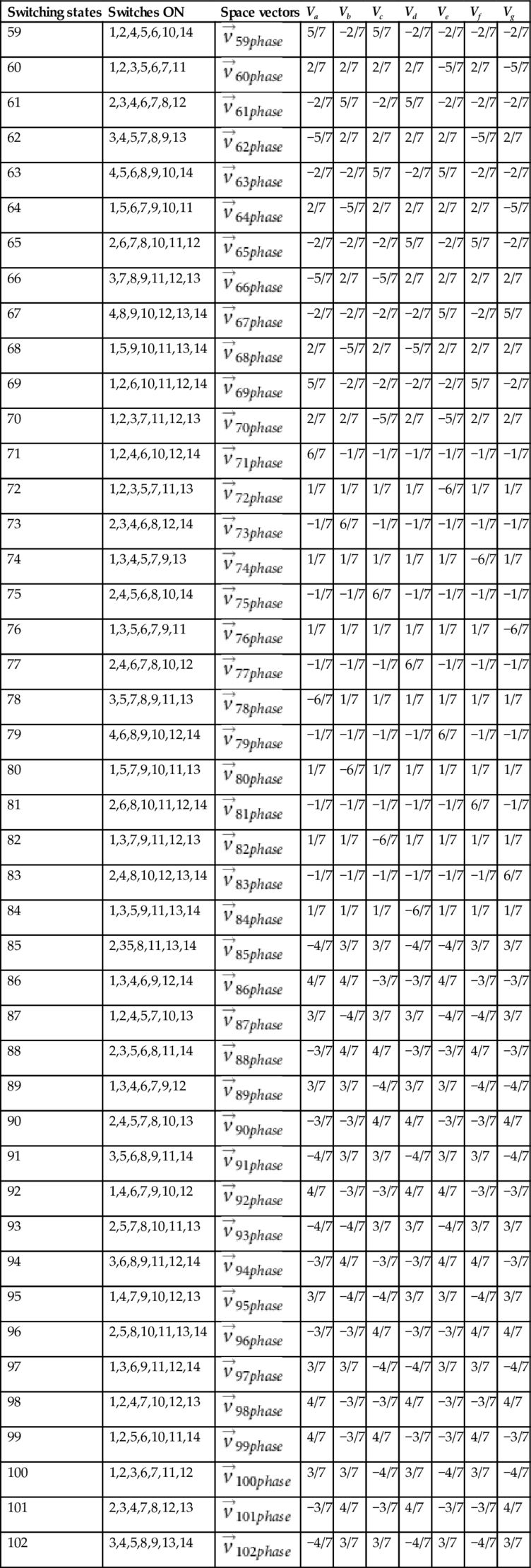
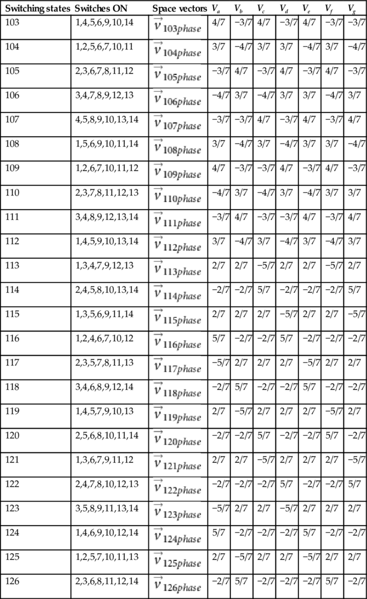
The phase voltage values are listed in Table 15.8, and the corresponding space vectors for 15–126 can be obtained using Eq. (15.105) and are given by expressions (15.126)–(15.133). The complete space-vector model of phase voltage is shown in Fig. 15.63.
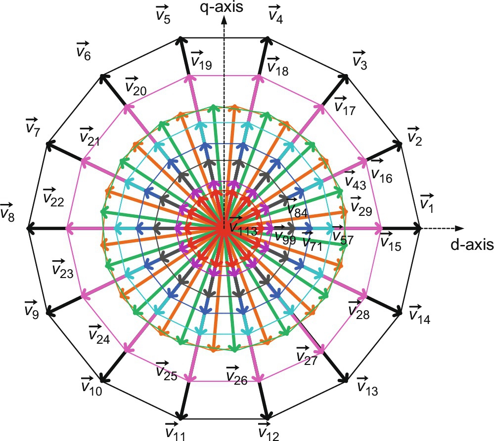
Table 15.8
Phase voltages (p.u.) values for PWM mode
| Switching states | Switches ON | Space vectors | Va | Vb | Vc | Vd | Ve | Vf | Vg |
| 15 | 1,2,3,5,11,13,14 | 2/7 | 2/7 | 2/7 | −5/7 | −5/7 | 2/7 | 2/7 | |
| 16 | 1,2,3,4,6,12,14 | 5/7 | 5/7 | −2/7 | −2/7 | −2/7 | −2/7 | −2/7 | |
| 17 | 1,2,3,4,5,7,13 | 2/7 | 2/7 | 2/7 | 2/7 | −5/7 | −5/7 | 2/7 | |
| 18 | 2,3,4,5,6,8,14 | −2/7 | 5/7 | 5/7 | −2/7 | −2/7 | −2/7 | −2/7 | |
| 19 | 1,3,4,5,6,7,9 | 2/7 | 2/7 | 2/7 | 2/7 | 2/7 | −5/7 | −5/7 | |
| 20 | 2,4,5,6,7,8,10 | −2/7 | −2/7 | 5/7 | 5/7 | −2/7 | −2/7 | −2/7 | |
| 21 | 3,5,6,7,8,9,11 | −5/7 | 2/7 | 2/7 | 2/7 | 2/7 | 2/7 | −5/7 | |
| 22 | 4,6,7,8,9,10,12 | −2/7 | −2/7 | −2/7 | 5/7 | 5/7 | −2/7 | −2/7 | |
| 23 | 5,7,8,9,10,11,13 | −5/7 | −5/7 | 2/7 | 2/7 | 2/7 | 2/7 | 2/7 | |
| 24 | 6,8,9,10,11,12,14 | −2/7 | −2/7 | −2/7 | −2/7 | 5/7 | 5/7 | −2/7 | |
| 25 | 7,9,10,11,12,13 | 2/7 | −5/7 | −5/7 | 2/7 | 2/7 | 2/7 | 2/7 | |
| 26 | 2,8,10,11,12,13,14 | −2/7 | −2/7 | −2/7 | −2/7 | −2/7 | 5/7 | 5/7 | |
| 27 | 1,3,9,11,12,13,14 | 2/7 | 2/7 | −5/7 | −5/7 | 2/7 | 2/7 | 2/7 | |
| 28 | 1,2,4,10,12,13,14 | 5/7 | −2/7 | −2/7 | −2/7 | −2/7 | −2/7 | 5/7 | |
| 29 | 1,2,4,5,10,13,14 | 4/7 | −3/7 | 4/7 | −3/7 | −3/7 | −3/7 | 4/7 | |
| 30 | 1,2,3,5,6,11,14 | 3/7 | 3/7 | 3/7 | −4/7 | −4/7 | 3/7 | −4/7 | |
| 31 | 1,2,3,4,6,7,12 | 4/7 | 4/7 | −3/7 | 4/7 | −3/7 | −3/7 | −3/7 | |
| 32 | 2,3,4,5,7,8,13 | −4/7 | 3/7 | 3/7 | 3/7 | −4/7 | −4/7 | 3/7 | |
| 33 | 3,4,5,6,8,9,14 | −3/7 | 4/7 | 4/7 | −3/7 | 4/7 | −3/7 | −3/7 | |
| 34 | 1,4,5,6,7,9,10 | 3/7 | −4/7 | 3/7 | 3/7 | 3/7 | −4/7 | −4/7 | |
| 35 | 2,5,6,7,8,10,11 | −3/7 | −3/7 | 4/7 | 4/7 | −3/7 | 4/7 | −3/7 | |
| 36 | 3,6,7,8,9,11,12 | −4/7 | 3/7 | −4/7 | 3/7 | 3/7 | 3/7 | −4/7 | |
| 37 | 4,7,8,9,10,12,13 | −3/7 | −3/7 | −3/7 | 4/7 | 4/7 | −3/7 | 4/7 | |
| 38 | 5,8,9,10,11,13,14 | −4/7 | −4/7 | 3/7 | −4/7 | −3/7 | −3/7 | −3/7 | |
| 39 | 1,6,9,10,11,12,14 | 4/7 | −3/7 | −3/7 | −3/7 | 4/7 | 4/7 | −3/7 | |
| 40 | 1,2,7,10,11,12,13 | 3/7 | −4/7 | −4/7 | 3/7 | −4/7 | 3/7 | 3/7 | |
| 41 | 2,3,8,11,12,13,14 | −3/7 | 4/7 | −3/7 | −3/7 | −3/7 | 4/7 | 4/7 | |
| 42 | 1,3,4,9,12,13,14 | 3/7 | 3/7 | −4/7 | −4/7 | 3/7 | −4/7 | 3/7 | |
| 43 | 1,2,3,4,7,12,13 | 3/7 | 3/7 | −4/7 | 3/7 | −4/7 | −4/7 | 3/7 | |
| 44 | 2,3,4,5,8,13,14 | −3/7 | 4/7 | 4/7 | −3/7 | −3/7 | −3/7 | 4/7 | |
| 45 | 1,3,4,5,6,9,14 | 3/7 | 3/7 | 3/7 | −4/7 | 3/7 | −4/7 | −4/7 | |
| 46 | 1,2,4,5,6,7,10 | 4/7 | −3/7 | 4/7 | 4/7 | −3/7 | −3/7 | −3/7 | |
| 47 | 2,3,5,6,7,8,11 | −4/7 | 3/7 | 3/7 | 3/7 | −4/7 | 3/7 | −4/7 | |
| 48 | 3,4,6,7,8,9,12 | −3/7 | 4/7 | −3/7 | 4/7 | 4/7 | −3/7 | −3/7 | |
| 49 | 4,5,7,8,9,10,13 | −4/7 | −4/7 | 3/7 | 3/7 | 3/7 | −4/7 | 3/7 | |
| 50 | 5,6,8,9,10,11,14 | −3/7 | −3/7 | 4/7 | −3/7 | 4/7 | 4/7 | −3/7 | |
| 51 | 1,6,7,9,10,11,12 | 3/7 | −4/7 | −4/7 | 3/7 | 3/7 | 3/7 | −4/7 | |
| 52 | 2,7,8,10,11,12,13 | −3/7 | −3/7 | −3/7 | 4/7 | −3/7 | 4/7 | 4/7 | |
| 53 | 3,8,9,11,12,13,14 | −4/7 | 3/7 | −4/7 | −4/7 | 3/7 | 3/7 | 3/7 | |
| 54 | 1,4,9,10,12,13,14 | 4/7 | −3/7 | −3/7 | −3/7 | 4/7 | −3/7 | 4/7 | |
| 55 | 1,2,5,10,1,13,14 | 3/7 | −4/7 | 3/7 | −4/7 | −4/7 | 3/7 | 3/7 | |
| 56 | 1,2,3,6,11,12,14 | 4/7 | 4/7 | −3/7 | −3/7 | −3/7 | 4/7 | −3/7 | |
| 57 | 2,3,4,8,12,13,14 | −2/7 | 5/7 | −2/7 | −2/7 | −2/7 | −2/7 | 5/7 | |
| 58 | 1,3,4,5,9,13,14 | 2/7 | 2/7 | 2/7 | −5/7 | 2/7 | −5/7 | 2/7 | |
| 59 | 1,2,4,5,6,10,14 | 5/7 | −2/7 | 5/7 | −2/7 | −2/7 | −2/7 | −2/7 | |
| 60 | 1,2,3,5,6,7,11 | 2/7 | 2/7 | 2/7 | 2/7 | −5/7 | 2/7 | −5/7 | |
| 61 | 2,3,4,6,7,8,12 | −2/7 | 5/7 | −2/7 | 5/7 | −2/7 | −2/7 | −2/7 | |
| 62 | 3,4,5,7,8,9,13 | −5/7 | 2/7 | 2/7 | 2/7 | 2/7 | −5/7 | 2/7 | |
| 63 | 4,5,6,8,9,10,14 | −2/7 | −2/7 | 5/7 | −2/7 | 5/7 | −2/7 | −2/7 | |
| 64 | 1,5,6,7,9,10,11 | 2/7 | −5/7 | 2/7 | 2/7 | 2/7 | 2/7 | −5/7 | |
| 65 | 2,6,7,8,10,11,12 | −2/7 | −2/7 | −2/7 | 5/7 | −2/7 | 5/7 | −2/7 | |
| 66 | 3,7,8,9,11,12,13 | −5/7 | 2/7 | −5/7 | 2/7 | 2/7 | 2/7 | 2/7 | |
| 67 | 4,8,9,10,12,13,14 | −2/7 | −2/7 | −2/7 | −2/7 | 5/7 | −2/7 | 5/7 | |
| 68 | 1,5,9,10,11,13,14 | 2/7 | −5/7 | 2/7 | −5/7 | 2/7 | 2/7 | 2/7 | |
| 69 | 1,2,6,10,11,12,14 | 5/7 | −2/7 | −2/7 | −2/7 | −2/7 | 5/7 | −2/7 | |
| 70 | 1,2,3,7,11,12,13 | 2/7 | 2/7 | −5/7 | 2/7 | −5/7 | 2/7 | 2/7 | |
| 71 | 1,2,4,6,10,12,14 | 6/7 | −1/7 | −1/7 | −1/7 | −1/7 | −1/7 | −1/7 | |
| 72 | 1,2,3,5,7,11,13 | 1/7 | 1/7 | 1/7 | 1/7 | −6/7 | 1/7 | 1/7 | |
| 73 | 2,3,4,6,8,12,14 | −1/7 | 6/7 | −1/7 | −1/7 | −1/7 | −1/7 | −1/7 | |
| 74 | 1,3,4,5,7,9,13 | 1/7 | 1/7 | 1/7 | 1/7 | 1/7 | −6/7 | 1/7 | |
| 75 | 2,4,5,6,8,10,14 | −1/7 | −1/7 | 6/7 | −1/7 | −1/7 | −1/7 | −1/7 | |
| 76 | 1,3,5,6,7,9,11 | 1/7 | 1/7 | 1/7 | 1/7 | 1/7 | 1/7 | −6/7 | |
| 77 | 2,4,6,7,8,10,12 | −1/7 | −1/7 | −1/7 | 6/7 | −1/7 | −1/7 | −1/7 | |
| 78 | 3,5,7,8,9,11,13 | −6/7 | 1/7 | 1/7 | 1/7 | 1/7 | 1/7 | 1/7 | |
| 79 | 4,6,8,9,10,12,14 | −1/7 | −1/7 | −1/7 | −1/7 | 6/7 | −1/7 | −1/7 | |
| 80 | 1,5,7,9,10,11,13 | 1/7 | −6/7 | 1/7 | 1/7 | 1/7 | 1/7 | 1/7 | |
| 81 | 2,6,8,10,11,12,14 | −1/7 | −1/7 | −1/7 | −1/7 | −1/7 | 6/7 | −1/7 | |
| 82 | 1,3,7,9,11,12,13 | 1/7 | 1/7 | −6/7 | 1/7 | 1/7 | 1/7 | 1/7 | |
| 83 | 2,4,8,10,12,13,14 | −1/7 | −1/7 | −1/7 | −1/7 | −1/7 | −1/7 | 6/7 | |
| 84 | 1,3,5,9,11,13,14 | 1/7 | 1/7 | 1/7 | −6/7 | 1/7 | 1/7 | 1/7 | |
| 85 | 2,35,8,11,13,14 | −4/7 | 3/7 | 3/7 | −4/7 | −4/7 | 3/7 | 3/7 | |
| 86 | 1,3,4,6,9,12,14 | 4/7 | 4/7 | −3/7 | −3/7 | 4/7 | −3/7 | −3/7 | |
| 87 | 1,2,4,5,7,10,13 | 3/7 | −4/7 | 3/7 | 3/7 | −4/7 | −4/7 | 3/7 | |
| 88 | 2,3,5,6,8,11,14 | −3/7 | 4/7 | 4/7 | −3/7 | −3/7 | 4/7 | −3/7 | |
| 89 | 1,3,4,6,7,9,12 | 3/7 | 3/7 | −4/7 | 3/7 | 3/7 | −4/7 | −4/7 | |
| 90 | 2,4,5,7,8,10,13 | −3/7 | −3/7 | 4/7 | 4/7 | −3/7 | −3/7 | 4/7 | |
| 91 | 3,5,6,8,9,11,14 | −4/7 | 3/7 | 3/7 | −4/7 | 3/7 | 3/7 | −4/7 | |
| 92 | 1,4,6,7,9,10,12 | 4/7 | −3/7 | −3/7 | 4/7 | 4/7 | −3/7 | −3/7 | |
| 93 | 2,5,7,8,10,11,13 | −4/7 | −4/7 | 3/7 | 3/7 | −4/7 | 3/7 | 3/7 | |
| 94 | 3,6,8,9,11,12,14 | −3/7 | 4/7 | −3/7 | −3/7 | 4/7 | 4/7 | −3/7 | |
| 95 | 1,4,7,9,10,12,13 | 3/7 | −4/7 | −4/7 | 3/7 | 3/7 | −4/7 | 3/7 | |
| 96 | 2,5,8,10,11,13,14 | −3/7 | −3/7 | 4/7 | −3/7 | −3/7 | 4/7 | 4/7 | |
| 97 | 1,3,6,9,11,12,14 | 3/7 | 3/7 | −4/7 | −4/7 | 3/7 | 3/7 | −4/7 | |
| 98 | 1,2,4,7,10,12,13 | 4/7 | −3/7 | −3/7 | 4/7 | −3/7 | −3/7 | 4/7 | |
| 99 | 1,2,5,6,10,11,14 | 4/7 | −3/7 | 4/7 | −3/7 | −3/7 | 4/7 | −3/7 | |
| 100 | 1,2,3,6,7,11,12 | 3/7 | 3/7 | −4/7 | 3/7 | −4/7 | 3/7 | −4/7 | |
| 101 | 2,3,4,7,8,12,13 | −3/7 | 4/7 | −3/7 | 4/7 | −3/7 | −3/7 | 4/7 | |
| 102 | 3,4,5,8,9,13,14 | −4/7 | 3/7 | 3/7 | −4/7 | 3/7 | −4/7 | 3/7 | |
| 103 | 1,4,5,6,9,10,14 | 4/7 | −3/7 | 4/7 | −3/7 | 4/7 | −3/7 | −3/7 | |
| 104 | 1,2,5,6,7,10,11 | 3/7 | −4/7 | 3/7 | 3/7 | −4/7 | 3/7 | −4/7 | |
| 105 | 2,3,6,7,8,11,12 | −3/7 | 4/7 | −3/7 | 4/7 | −3/7 | 4/7 | −3/7 | |
| 106 | 3,4,7,8,9,12,13 | −4/7 | 3/7 | −4/7 | 3/7 | 3/7 | −4/7 | 3/7 | |
| 107 | 4,5,8,9,10,13,14 | −3/7 | −3/7 | 4/7 | −3/7 | 4/7 | −3/7 | 4/7 | |
| 108 | 1,5,6,9,10,11,14 | 3/7 | −4/7 | 3/7 | −4/7 | 3/7 | 3/7 | −4/7 | |
| 109 | 1,2,6,7,10,11,12 | 4/7 | −3/7 | −3/7 | 4/7 | −3/7 | 4/7 | −3/7 | |
| 110 | 2,3,7,8,11,12,13 | −4/7 | 3/7 | −4/7 | 3/7 | −4/7 | 3/7 | 3/7 | |
| 111 | 3,4,8,9,12,13,14 | −3/7 | 4/7 | −3/7 | −3/7 | 4/7 | −3/7 | 4/7 | |
| 112 | 1,4,5,9,10,13,14 | 3/7 | −4/7 | 3/7 | −4/7 | 3/7 | −4/7 | 3/7 | |
| 113 | 1,3,4,7,9,12,13 | 2/7 | 2/7 | −5/7 | 2/7 | 2/7 | −5/7 | 2/7 | |
| 114 | 2,4,5,8,10,13,14 | −2/7 | −2/7 | 5/7 | −2/7 | −2/7 | −2/7 | 5/7 | |
| 115 | 1,3,5,6,9,11,14 | 2/7 | 2/7 | 2/7 | −5/7 | 2/7 | 2/7 | −5/7 | |
| 116 | 1,2,4,6,7,10,12 | 5/7 | −2/7 | −2/7 | 5/7 | −2/7 | −2/7 | −2/7 | |
| 117 | 2,3,5,7,8,11,13 | −5/7 | 2/7 | 2/7 | 2/7 | −5/7 | 2/7 | 2/7 | |
| 118 | 3,4,6,8,9,12,14 | −2/7 | 5/7 | −2/7 | −2/7 | 5/7 | −2/7 | −2/7 | |
| 119 | 1,4,5,7,9,10,13 | 2/7 | −5/7 | 2/7 | 2/7 | 2/7 | −5/7 | 2/7 | |
| 120 | 2,5,6,8,10,11,14 | −2/7 | −2/7 | 5/7 | −2/7 | −2/7 | 5/7 | −2/7 | |
| 121 | 1,3,6,7,9,11,12 | 2/7 | 2/7 | −5/7 | 2/7 | 2/7 | 2/7 | −5/7 | |
| 122 | 2,4,7,8,10,12,13 | −2/7 | −2/7 | −2/7 | 5/7 | −2/7 | −2/7 | 5/7 | |
| 123 | 3,5,8,9,11,13,14 | −5/7 | 2/7 | 2/7 | −5/7 | 2/7 | 2/7 | 2/7 | |
| 124 | 1,4,6,9,10,12,14 | 5/7 | −2/7 | −2/7 | −2/7 | 5/7 | −2/7 | −2/7 | |
| 125 | 1,2,5,7,10,11,13 | 2/7 | −5/7 | 2/7 | 2/7 | −5/7 | 2/7 | 2/7 | |
| 126 | 2,3,6,8,11,12,14 | −2/7 | 5/7 | −2/7 | −2/7 | −2/7 | 5/7 | −2/7 |

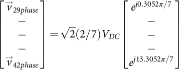
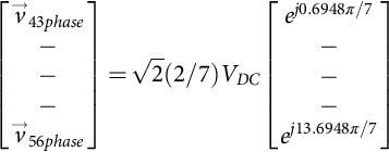


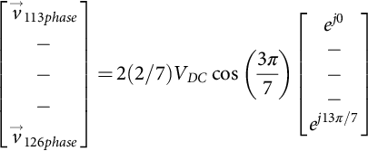
It can be seen that the total of 128 space vectors, available in the PWM operation, fall into 10 distinct categories regarding the magnitude of the available output phase voltages. The phase voltage space vectors are summarized in Table 15.9 for all 128 switching states including 14-step operation.
Table 15.9
Phase-to-neutral voltage space vectors for states 1–128
| Space vectors | Set number in planes | Value of the space vectors in d-q plane | ||
| d-q | x1-y1 | x2-y2 | ||
| v1phase to v14phase | 1 | 8 | 7 | |
| v15phase to v28phase | 2 | 5 | 9 | |
| v29phase to v42phase | 3 | 3 | 4 | |
| v43phase to v56phase | 4 | 4 | 3 | |
| v57phase to v70phase | 5 | 9 | 2 | |
| v71phase to v84phase | 6 | 6 | 6 | |
| v85phase to v98phase | 7 | 1 | 8 | |
| v99phase to v112phase | 8 | 7 | 1 | |
| v113phase to v126phase | 9 | 2 | 5 | |
| v127phase to v128phase | – | – | – | 0 |
