
AC-AC Converters
Mohammad Ali Aligarh Muslim University, Aligarh, India
Atif Iqbal Qatar University, Doha, Qatar
Mohammad Rizwan Khan Aligarh Muslim University, Aligarh, India
Abstract
Ac-ac converters broadly define a set of power electronic topologies that are employed to obtain ac output of variable amplitude and frequency from fixed ac input without employment of bulky reactive components. A converter that gives variable amplitude ac is known as a voltage controller and that employed for variable-frequency ac is known as cycloconverter. Depending on the operation of thyristors, cycloconverters can be naturally commutated (NCC) or forcefully commutated (FCC). Variation of the frequency in the NCC is restricted to only half of the supply frequency. In contrast, FCC is employed for unrestricted frequency change but with less voltage transfer ratio. Matrix converter (MC) is a kind of FCC that employs fast switching bidirectional switches and is of two types, namely, direct (DMC) and indirect MC (IMC). New topologies in the field of MCs are multilevel MC, multimodular MC, and sparse MCs. Z-source DMC and IMC are considered as it boosts up in the voltage transfer ratio and reduces the commutation problems.
Keywords
Ac-ac conversion; Ac voltage controller; Frequency changer; Cycloconverter; Matrix converter
14.1 Introduction
A power electronic ac-ac converter, in generic form, accepts electric power from one system and converts it for delivery to another ac system with waveforms of different amplitude, frequency, and phase. Conventionally, the input system is of single-phase or three-phase type depending on the power ratings of the load, and the output system is of single-phase or three-phase type. However, recent research trend shows considerable orientation toward multiphase systems as they exhibit decrement in time and space harmonics, reduction in per phase current, increment in fault tolerance and reliability, etc. The ac-ac converters employed to vary the rms voltage across the load at constant frequency are known as ac voltage controllers or ac regulators. The voltage control is accomplished either by (1) phase control under natural commutation using pairs of silicon-controlled rectifiers (SCRs) or triacs or (2) by on/off control under forced commutation/self-commutation using fully controlled self-commutated switches, such as gate turn-off thyristors (GTOs), power transisto/rs, integrated-gate bipolar transistor (IGBTs), MOS-controlled thyristors (MCTs), and integrated-gate-commutated thyristor (IGCTs). Employment of switches depends on the power that is to be delivered (and thus on the switching frequency range of the device). The ac-ac power converters in which ac power at one frequency is directly converted to ac power at another frequency without any intermediate dc conversion link (as in the case of conventionally employed rectifier-inverter or back-to-back configurations) are known as cycloconverters, the majority of which uses naturally commutated SCRs for their operation when the maximum output frequency is limited to a fraction of the input frequency. With rapid advancements of fast-acting fully controlled switches, forced commutated cycloconverters, or matrix converters with bidirectional on/off control switches provide independent control of the magnitude and the frequency of the generated output voltage, as well as sinusoidal modulation of output voltage and current.
Although typical applications of ac voltage controllers include lighting and heating control, online transformer tap changing, soft starting, and speed control of pump and fan drives, the cycloconverters are mainly used for high-power, low-speed, large ac motor drives for application in cement kilns, rolling mills, and ship propellers. The power circuits, control methods, and the operation of the ac voltage controllers, cycloconverters, and matrix converters are introduced in this chapter. A brief review is also made regarding their applications.
14.2 Single-Phase AC-AC Voltage Controller
The basic power circuit of a single-phase ac-ac voltage controller, as shown in Fig. 14.1A, comprises a pair of SCRs connected back-to-back (also known as inverse-parallel or antiparallel) between the ac supply and the load. This connection provides a bidirectional full-wave symmetrical control, and the SCR pair can be replaced by a triac (Fig. 14.1B) for low-power applications. Alternate arrangements are shown in Fig. 14.1C with two diodes and two SCRs to provide a common cathode connection for simplifying the gating circuit without requiring isolation and in Fig. 14.1D with one SCR and four diodes to reduce the device cost but with increased device conduction loss. An SCR and diode combination known as thyrode controller, as shown in Fig. 14.1E, provides a unidirectional half-wave asymmetrical voltage control with device economy but introduces dc component and more harmonics, and thus, it is not so practical to use except for very low-power-heating load.
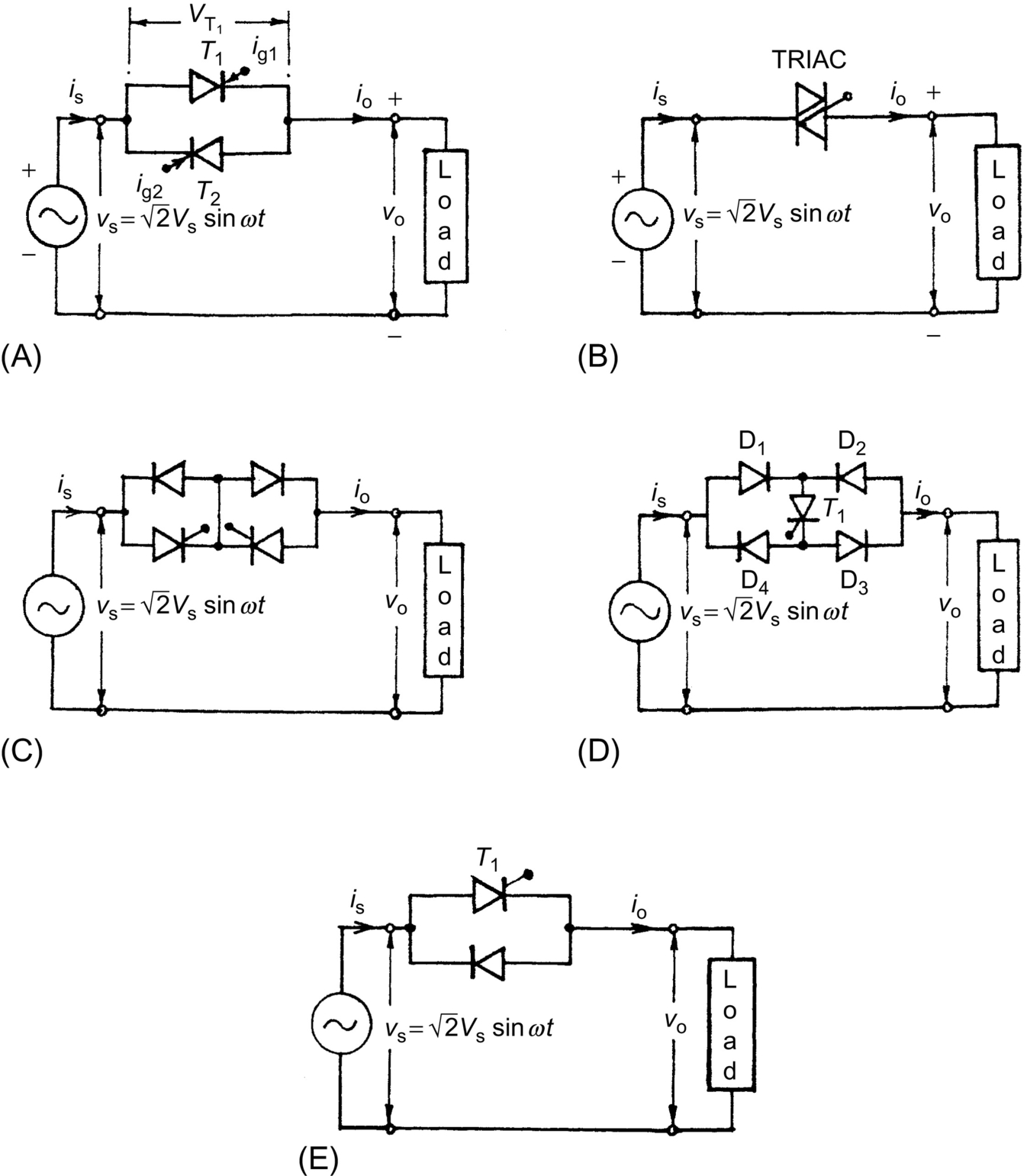
With phase control, the switches conduct the load current for a chosen period of each input cycle of voltage, and with on/off control, either the switches connect the load for a few cycles of input voltage and disconnect it for the next few cycles (integral cycle control) or the switches are turned on and off several times within alternate half cycles of input voltage (ac chopper or pulse-width modulated (PWM) ac voltage controller).
14.2.1 Phase-Controlled Single-Phase AC Voltage Controller
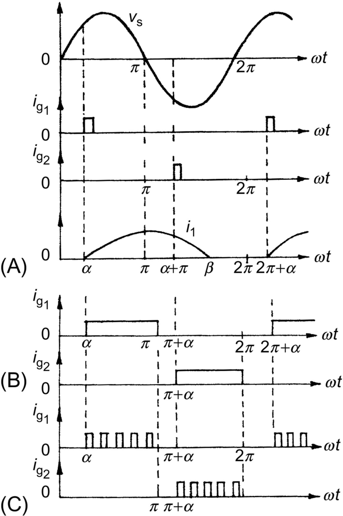
For a full-wave symmetrical phase control, the SCRs T1 and T2 in Fig. 14.1A are gated at α and π+α, respectively, from the zero crossing of the input voltage; by varying α, the power flow to the load is controlled through voltage control in alternate half cycles. As long as one SCR is carrying current, the other SCR remains reverse-biased by the voltage drop across the conducting SCR. The principle of operation in each half cycle is similar to that of the controlled half-wave rectifier, and one can use the same approach for analysis of the circuit.
Operation with R-load. Fig. 14.2 shows the typical voltage and current waveforms for the single-phase bidirectional phase-controlled ac voltage controller of Fig. 14.1A with a resistive load. The output voltage and current waveforms have half-wave symmetry and so no dc component.

If vs=√2Vssinωt![]() is the source voltage, the rms output voltage with T1 triggered at α can be found from the half-wave symmetry as
is the source voltage, the rms output voltage with T1 triggered at α can be found from the half-wave symmetry as
Vo=[1ππ∫α2V2ssin2ωtd(ωt)]12=Vs[1−απ+sin2α2π]12

Note that Vo can be varied from Vs to 0 by varying α from 0 to π:
Thermsvalueofloadcurrent,Io=VoR

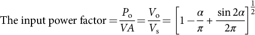
Theinputpowerfactor=PoVA=VoVs=[1−απ+sin2α2π]12
TheaverageSCRcurrent,IA,SCR=12πRπ∫α√2Vssinωtd(ωt)

Since each SCR carries half the line current, the rms current in each SCR is
Io,SCR=Io√2

Operation with RL Load. Fig. 14.3 shows the voltage and current waveforms for the controller in Fig. 14.1A with RL load. Due to the inductance, the current carried by the SCR T1 may not fall to zero at ωt=π![]() when the input voltage goes negative and may continue till ωt=β
when the input voltage goes negative and may continue till ωt=β![]() , the extinction angle, as shown. The conduction angle,
, the extinction angle, as shown. The conduction angle,

θ=β−α
of the SCR depends on the firing delay angle α and the load impedance angle ϕ.
The expression for the load current Io(ωt), when conducting from α to β, can be derived in the same way as that used for a phase-controlled rectifier in a discontinuous mode by solving the relevant Kirchhoff's voltage equation:
io(ωt)=√2VZ[sin(ωt−ϕ)−sin(α−ϕ)e(α−ωt)/tanϕ],α<ωt<β
where Z=(R2+ω2L2)12=loadimpedance![]() and ϕ=loadimpedanceangle=tan−1(ωL/R)
and ϕ=loadimpedanceangle=tan−1(ωL/R)![]() .
.
The angle β, when the current io falls to zero, can be determined from the following transcendental equation resulted by using io(ωt=β)=0![]() in Eq. (14.7):
in Eq. (14.7):
sin(β−ϕ)=sin(α−ϕ)−sin(α−ϕ)e(α−β)/tanϕ
From Eqs. (14.6) and (14.8), one can obtain a relationship between θ and α for a given value of ϕ, as shown in Fig. 14.4, which shows that as α is increased, the conduction angle θ decreases, and thus, the rms value of the current decreases.

The rms output voltage
Vo=[1πβ∫α2V2ssin2ωtd(ωt)]12=Vsπ[β−α+sin2α2−sin2β2]12

Vo can be evaluated for two possible extreme values of ϕ=0![]() when β=π
when β=π![]() , and ϕ=π/2
, and ϕ=π/2![]() when β=2π−α
when β=2π−α![]() , and the envelope of the voltage control characteristics for this controller is shown in Fig. 14.5.
, and the envelope of the voltage control characteristics for this controller is shown in Fig. 14.5.

The rms SCR current can be obtained from Eq. (14.7) as follows:
Io,SCR=[12πβ∫αi2od(ωt)]12
Thermsloadcurrent,Io=√2Io,SCR
TheaveragevalueofSCRcurrent,IA,SCR=12πβ∫αiod(ωt)

Gating Signal Requirements. For the inverse-parallel SCRs as shown in Fig. 14.1A, the gating signals of SCRs must be isolated from one another because there is no common cathode. For R-load, each SCR stops conducting at the end of each half cycle and under this condition, single short pulses may be used for gating as shown in Fig. 14.2. With RL load, however, this single short pulse gating is not suitable as shown in Fig. 14.6. When SCR T2 is triggered at ωt=π+α![]() , SCR T1 is still conducting due to the load inductance. By the time the SCR T1 stops conducting at β, the gate pulse for SCR T2 has already ceased and T2 will fail to turn on resulting the converter to operate as a single-phase rectifier with conduction of T1 only. This necessitates the application of a sustained gate pulse in the form of either a continuous signal for the half-cycle period or better a train of pulses (carrier frequency gating) as the former results in increased dissipation in SCR gate circuit, and a large isolating pulse transformer is required.
, SCR T1 is still conducting due to the load inductance. By the time the SCR T1 stops conducting at β, the gate pulse for SCR T2 has already ceased and T2 will fail to turn on resulting the converter to operate as a single-phase rectifier with conduction of T1 only. This necessitates the application of a sustained gate pulse in the form of either a continuous signal for the half-cycle period or better a train of pulses (carrier frequency gating) as the former results in increased dissipation in SCR gate circuit, and a large isolating pulse transformer is required.
Operation with α<ϕ![]() . If α=ϕ
. If α=ϕ![]() , then from Eq. (14.8),
, then from Eq. (14.8),
sin(β−ϕ)=sin(β−α)=0
and
β−α=θ=π
As the conduction angle θ cannot exceed π and the load current must pass through zero, the control range of the firing angle is ϕ≤α≤π![]() . With narrow gating pulses and α<ϕ
. With narrow gating pulses and α<ϕ![]() , only one SCR will conduct resulting in a rectifier action as shown. Even with a train of pulses, if α<ϕ
, only one SCR will conduct resulting in a rectifier action as shown. Even with a train of pulses, if α<ϕ![]() , the changes in the firing angle will not change the output voltage and current but both the SCRs will conduct for the period π with T1 becoming on at ωt=π
, the changes in the firing angle will not change the output voltage and current but both the SCRs will conduct for the period π with T1 becoming on at ωt=π![]() and T2 at ωt+π
and T2 at ωt+π![]() .
.
The duration of this dead zone (α=0![]() to ϕ), which varies with the load impedance angle ϕ, is not a desirable feature in closed-loop control schemes. An alternative approach to the phase control with respect to the input voltage zero crossing has been visualized in which the firing angle is defined with respect to the instant when it is the load current, not the input voltage, that reaches zero, this angle being called the hold-off angle (γ) or the control angle (as marked in Fig. 14.3). This method needs sensing the load current, which may otherwise be required in a closed-loop controller for monitoring or control purposes.
to ϕ), which varies with the load impedance angle ϕ, is not a desirable feature in closed-loop control schemes. An alternative approach to the phase control with respect to the input voltage zero crossing has been visualized in which the firing angle is defined with respect to the instant when it is the load current, not the input voltage, that reaches zero, this angle being called the hold-off angle (γ) or the control angle (as marked in Fig. 14.3). This method needs sensing the load current, which may otherwise be required in a closed-loop controller for monitoring or control purposes.
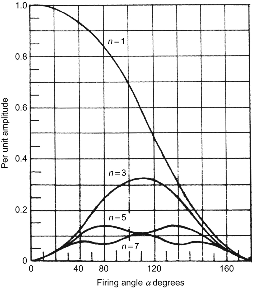
Power Factor and Harmonics. As in the case of phase-controlled rectifiers, the important limitations of the phase-controlled ac voltage controllers are the poor power factor and the introduction of harmonics in the source currents. As seen from Eq. (14.3), the input power factor depends on α, and as α increases, the power factor decreases.
The harmonic distortion increases and the quality of the input current decreases with increase of firing angle. The variations of low-order harmonics with the firing angle as computed by Fourier analysis of the voltage waveform of Fig. 14.2 (with R-load) are shown in Fig. 14.7. Only odd harmonics exist in the input current because of half-wave symmetry.
14.2.2 Single-Phase AC-AC Voltage Controller with On/Off Control
Integral Cycle Control. As an alternative to the phase control, the method of integral cycle control or burst firing is used for systems with large time constants, for example, heating loads. Here, the switch is turned on for a time tn with n integral cycles and turned off for a time tm with m integral cycles (Fig. 14.8). As the SCRs or triacs used here are turned on at the zero crossing of the input voltage and turn off occurs at zero current, supply harmonics and radio-frequency interference are very low.

However, subharmonic frequency components may be generated, which are undesirable because they may set up subharmonic resonance in the power supply system, cause lamp flicker, and may interfere with the natural frequencies of motor loads causing shaft oscillations.
For sinusoidal input voltage, v=√2Vssinωt![]() , the rms output voltage
, the rms output voltage
Vo=Vs√kwherek=n/(n+m)=dutycycleandVs=rmsphasevoltage

Thepowerfactor=√k
which is poorer for lower values of the duty cycle k.
PWM AC Chopper. As in the case of controlled rectifier, the performance of ac voltage controllers can be improved in terms of harmonics, quality of output current, and input power factor by PWM control in PWM ac choppers; the circuit configuration of one such single-phase unit is shown in Fig. 14.9. Here, fully controlled switches S1 and S2 connected in antiparallel are turned on and off many times during the positive and negative half cycles of the input voltage, respectively. S1′ and S2′ provide the freewheeling paths for the load current when S1 and S2 are off. An input capacitor filter may be provided to attenuate the high switching frequency currents drawn from the supply and also to improve the input power factor. Fig. 14.10 shows the typical output voltage and load current waveform for a single-phase PWM ac chopper. It can be shown that the control characteristics of an ac chopper depend on the modulation index M, which theoretically varies from 0 to 1.


Three-phase PWM choppers consist of three single-phase choppers connected in either delta or four-wire (star) configuration.
14.3 Three-Phase AC-AC Voltage Controllers
14.3.1 Phase-Controlled Three-Phase AC Voltage Controllers
Various Configurations. Several possible circuit configurations for three-phase phase-controlled ac regulators with star- or delta-connected loads are shown in Fig. 14.11A–H.

The configurations in (A) and (B) can be realized by three single-phase ac regulators operating independently of each other, and they are easy to analyze. In (A), the SCRs are to be rated to carry line currents and withstand phase voltages, whereas in (B) they should be capable to carry phase currents and withstand the line voltage. In (B), the line currents are free from triplen harmonics while these are present in the closed delta. The power factor in (B) is slightly higher. The firing angle control range for both these circuits is 0–180 degrees for R-load.
The circuits in (C) and (D) are three-phase three-wire circuits and are complicated to analyze. In both these circuits, at least two SCRs, one in each phase, must be gated simultaneously to get the controller started by establishing a current path between the supply lines. This necessitates two firing pulses spaced at 60 degrees apart per cycle for firing each SCR. The operation modes are defined by the number of SCRs conducting in these modes. The firing control range is 0–150 degrees. The triplen harmonics are absent in both these configurations.
Another configuration is shown in (E) when the controllers are connected in delta and the load is connected between the supply and the converter. Here, current can flow between two lines even if one SCR is conducting so each SCR requires one firing pulse per cycle. The voltage and current ratings of SCRs are nearly the same as that of the circuit (B). It is also possible to reduce the number of devices to three SCRs in delta as shown in (F), connecting one source terminal directly to one load circuit terminal. Each SCR is provided with gate pulses in each cycle spaced at 120 degrees apart. In both (E) and (F), each end of each phase must be accessible. The number of devices in (F) is less, but their current ratings must be higher.
As in the case of single-phase phase-controlled voltage regulator, the total regulator cost can be reduced by replacing six SCRs by three SCRs and three diodes, resulting in three-phase half-wave controlled unidirectional ac regulators as shown in (G) and (H) for star- and delta-connected loads. The main drawback of these circuits is the large harmonic content in the output voltage—particularly, the second harmonic because of the asymmetry. However, the dc components are absent in the line. The maximum firing angle in the half-wave controlled regulator is 210 degrees.
14.3.2 Fully Controlled Three-Phase Three-Wire AC Voltage Controller
Star-connected Load with Isolated Neutral. The analysis of operation of the full-wave controller with isolated neutral as shown in Fig. 14.11C is, as mentioned, quite complicated in comparison with that of a single-phase controller, particularly for an RL or motor load. As a simple example, the operation of this controller with a simple star-connected R-load is considered here. The six SCRs are turned on in the sequence 1-2-3-4-5-6 at 60 degrees intervals, and the gate signals are sustained throughout the possible conduction angle.
The output phase voltage waveforms for α=30, 75, and 120 degrees for a balanced three-phase R-load are shown in Fig. 14.12. At any interval, either three SCRs or two SCRs or no SCRs may be on, and the instantaneous output voltages to the load are either a line-to-neutral voltage (three SCRs on) or one-half of the line-to-line voltage (two SCRs on) or zero (no SCR on).

 , (B) van for α=75°
 , and (C) van=120°
 .
.Depending on the firing angle α, there may be three operating modes:
Mode I (also known as Mode 2/3). 0 degrees≤α≤60 degrees; There are periods when three SCRs are conducting, one in each phase for either direction, and there are periods when just two SCRs conduct.
For example, with α=30 degrees in Fig. 14.12A, assume that at ωt=0![]() , SCRs T5 and T6 are conducting, and the current through the R-load in a-phase is zero making van=0
, SCRs T5 and T6 are conducting, and the current through the R-load in a-phase is zero making van=0![]() . At ωt=30degrees
. At ωt=30degrees![]() , T1 receives a gate pulse and starts conducting; T5 and T6 remain on, and van=vAN
, T1 receives a gate pulse and starts conducting; T5 and T6 remain on, and van=vAN![]() . The current in T5 reaches zero at 60 degrees, turning T5 off. With T1 and T6 staying on, van=12vAB
. The current in T5 reaches zero at 60 degrees, turning T5 off. With T1 and T6 staying on, van=12vAB![]() . At 90 degrees, T2 is turned on, the three SCRs T1, T2, and T6 are then conducting, and van=vAN
. At 90 degrees, T2 is turned on, the three SCRs T1, T2, and T6 are then conducting, and van=vAN![]() . At 120 degrees, T6 turns off, leaving T1 and T2 on, so van=12vAC
. At 120 degrees, T6 turns off, leaving T1 and T2 on, so van=12vAC![]() . Thus, with the progress of firing in sequence till α=60 degrees, the number of SCRs conducting at a particular instant alternates between two and three.
. Thus, with the progress of firing in sequence till α=60 degrees, the number of SCRs conducting at a particular instant alternates between two and three.
Mode II (also known as Mode 2/2). 60 degrees≤α≤90 degrees; Two SCRs, one in each phase, always conduct.
For α=75 degrees as shown in Fig. 14.12B, just prior to α=75 degrees, SCRs T5 and T6 were conducting, and van=0![]() . At 75 degrees, T1 is turned on, and T6 continues to conduct, whereas T5 turns off as vCN is negative. van=12vAB
. At 75 degrees, T1 is turned on, and T6 continues to conduct, whereas T5 turns off as vCN is negative. van=12vAB![]() . When T2 is turned on at 135 degrees, T6 is turned off, and van=12vAC
. When T2 is turned on at 135 degrees, T6 is turned off, and van=12vAC![]() . The next SCR to turn on is T3, which turns off T1, and van=0
. The next SCR to turn on is T3, which turns off T1, and van=0![]() . One SCR is always turned off when another is turned on in this range of α, and the output voltage is either one-half line-to-line voltage or zero.
. One SCR is always turned off when another is turned on in this range of α, and the output voltage is either one-half line-to-line voltage or zero.
Mode III (also known as Mode 0/2). 90 degrees≤α≤150 degrees, when none or two SCRs conduct.
For α=120 degrees, Fig. 14.12C, earlier, no SCRs were on, and van=0![]() . At α=120 degrees, SCR T1 is given a gate signal, whereas T6 has a gate signal already applied. Since vAB is positive, T1 and T6 are forward-biased, and they begin to conduct, and van=12vAB
. At α=120 degrees, SCR T1 is given a gate signal, whereas T6 has a gate signal already applied. Since vAB is positive, T1 and T6 are forward-biased, and they begin to conduct, and van=12vAB![]() . Both T1 and T6 turn off when vAB becomes negative. When a gate signal is given to T2, it turns on, and T1 turns on again.
. Both T1 and T6 turn off when vAB becomes negative. When a gate signal is given to T2, it turns on, and T1 turns on again.
For α>150 degrees, there is no period when two SCRs are conducting and the output voltage is zero at α=150 degrees. Thus, the range of the firing angle control is 0 degrees≤α≤150 degrees.
For star-connected R-load, assuming the instantaneous phase voltages as
vAN=√2VssinωtvBN=√2Vssinωt−120degreesvCN=√2Vssinωt−240degrees

the expressions for the rms output phase voltage Vo can be derived for the three modes as follows:
0degrees≤α≤60degreesVo=Vs[1−3α2π+34πsin2α]12

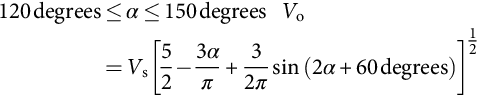
60degrees≤α≤90degreesVo=Vs[12+34πsin2α+sin(2α+60degrees)]12

90degrees≤α≤150degreesVo=Vs[54−3α2π+34πsin(2α+60degrees)]12

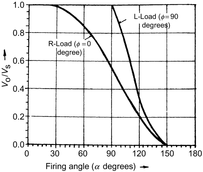
For star-connected pure L-load, the effective control starts at α>90 degrees, and the expressions for two ranges of α are as follows:
90degrees≤α≤120degreesVo=Vs[52−3απ+32πsin2α]12

120degrees≤α≤150degreesVo=Vs[52−3απ+32πsin(2α+60degrees)]12
The control characteristics for these two limiting cases (ϕ=0 for R-load and ϕ=90 degrees for L-load) are shown in Fig. 14.13. Here also, like the single-phase case, the dead zone may be avoided by controlling the voltage with respect to the control angle or hold-off angle (γ) from the zero crossing of current in place of the firing angle α.
RL Load. The analysis of the three-phase voltage controller with star-connected RL load with isolated neutral is quite complicated, since the SCRs do not cease to conduct at voltage zero, and the extinction angle β is to be known by solving the transcendental equation for the case. In this case, the mode II operation disappears [1], and the operation shift from mode I to mode III depends on the so-called critical angle αcrit [2,3], which can be evaluated from a numerical solution of the relevant transcendental equations. Computer simulation by either PSPICE program [4,5] or switching-variable approach coupled with an iterative procedure [6] is a practical means of obtaining the output voltage waveform in this case. Fig. 14.14 shows typical simulation results using the later approach [6] for a three-phase voltage controller-fed RL load for α=60, 90, and 105 degrees, which agree with the corresponding practical oscillograms given in [7].

 ) for
) for  , 90°, and 105°.
Delta-Connected R-Load. The configuration is shown in Fig. 14.11B. The voltage across an R-load is the corresponding line-to-line voltage when one SCR in that phase is on. Fig. 14.15 shows the line and phase currents for α=130 and 90 degrees with an R-load. The firing angle α is measured from the zero crossing of the line-to-line voltage, and the SCRs are turned on in the sequence as they are numbered. As in the single-phase case, the range of firing angle is ![]() degrees. The line currents can be obtained from the phase currents as follows:
degrees. The line currents can be obtained from the phase currents as follows:

 and (B)
  .
.

The line currents depend on the firing angle and may be discontinuous as shown. Due to the delta connection, the triplen harmonic currents flow around the closed delta and do not appear in the line. The rms value of the line current varies between the range
as the conduction angle varies from very small (large α) to 180 degrees (![]() ).
).
14.4 Cycloconverters
In contrast to the ac voltage controllers operating at constant frequency discussed so far, a cycloconverter operates as a direct ac-ac frequency changer with inherent voltage control feature. The basic principle of this converter to construct an alternating voltage wave of lower frequency from successive segment of voltage waves of higher frequency ac supply by a switching arrangement was conceived and patented in the 1920s. Grid-controlled mercury-arc rectifiers were used in these converters installed in Germany in the 1930s to obtain ![]() single-phase supply for ac series traction motors from a three-phase 50 Hz system, while at the same time, a cycloconverter using 18 thyratrons supplying a 400 hp synchronous motor was in operation for some years as a power station auxiliary drive in the United States. However, the practical and commercial utilization of these schemes waited till the SCRs became available in the 1960s. With the development of large-power SCRs and microprocessor-based control, the cycloconverter today is a matured practical converter for application in large-power low-speed variable-voltage variable-frequency (VVVF) ac drives in cement and steel rolling mills and in variable-speed constant-frequency (VSCF) systems in aircrafts and naval ships.
single-phase supply for ac series traction motors from a three-phase 50 Hz system, while at the same time, a cycloconverter using 18 thyratrons supplying a 400 hp synchronous motor was in operation for some years as a power station auxiliary drive in the United States. However, the practical and commercial utilization of these schemes waited till the SCRs became available in the 1960s. With the development of large-power SCRs and microprocessor-based control, the cycloconverter today is a matured practical converter for application in large-power low-speed variable-voltage variable-frequency (VVVF) ac drives in cement and steel rolling mills and in variable-speed constant-frequency (VSCF) systems in aircrafts and naval ships.
A cycloconverter is a naturally commuted converter with inherent capability of bidirectional power flow, and there is no real limitation on its size unlike an SCR inverter with commutation elements. Here, the switching losses are considerably low, the regenerative operation at full power over complete speed range is inherent and it delivers a nearly sinusoidal waveform resulting in minimum torque pulsation and harmonic heating effects. It is capable of operating even with blowing out of individual SCR fuse (unlike inverter), and the requirements regarding turn-off time, current rise time, and dv/dt sensitivity of SCRs are low. The main limitations of a naturally commutated cycloconverter are (1) limited frequency range for subharmonic free and efficient operation and (2) poor input displacement/power factor, particularly at low-output voltages.
14.4.1 Single-Phase to Single-Phase Cycloconverter
Though rarely used, the operation of a single-phase to single-phase cycloconverter is useful to demonstrate the basic principle involved. Fig. 14.16A shows the power circuit of a single-phase bridge type of cycloconverter, which has the same arrangement as that of a single-phase dual converter. The firing angles of the individual two-pulse two-quadrant bridge converters are continuously modulated here, so that each ideally produces the same fundamental ac voltage at its output terminals as marked in the simplified equivalent circuit in Fig. 14.16B. Because of the unidirectional current-carrying property of the individual converters, it is inherent that the positive half cycle of the current is carried by the P-converter and the negative half cycle of the current by the N-converter regardless of the phase of the current with respect to the voltage. This means that for a reactive load, each converter operates in both rectifying and inverting region during the period of the associated half cycle of the low-frequency output current.

Operation with R-Load. Fig. 14.17 shows the input and output voltage waveforms with a pure R-load for a ![]() cycloconverter. The P- and N-converters operate for alternate To/2 periods. The output frequency (1/To) can be varied by varying To and the voltage magnitude by varying the firing angle α of the SCRs. As shown in the figure, three cycles of the ac input wave are combined to produce one cycle of the output frequency to reduce the supply frequency to one-third across the load.
cycloconverter. The P- and N-converters operate for alternate To/2 periods. The output frequency (1/To) can be varied by varying To and the voltage magnitude by varying the firing angle α of the SCRs. As shown in the figure, three cycles of the ac input wave are combined to produce one cycle of the output frequency to reduce the supply frequency to one-third across the load.

 cycloconverter with RL load.
If αP is the firing angle of the P-converter, the firing angle of the N-converter αN is ![]() , and the average voltage of the P-converter is equal and opposite to that of the N-converter.
, and the average voltage of the P-converter is equal and opposite to that of the N-converter.
The inspection of Fig. 14.17 shows that the waveform with α remaining fixed in each half cycle generates a square wave having a large low-order harmonic content. A near approximation to sine wave can be synthesized by a phase modulation of the firing angles as shown in Fig. 14.18 for a 50–10 Hz cycloconverter. The harmonics in the load voltage waveform are less compared with earlier waveform. The supply current, however, contains a subharmonic at the output frequency for this case as shown.

Operation with RL Load. The cycloconverter is capable of supplying loads of any power factor. Fig. 14.19 shows the idealized output voltage and current waveforms for a lagging power factor load where both the converters are operating as rectifier and inverter at the intervals marked. The load current lags the output voltage, and the load current direction determines which converter is conducting. Each converter continues to conduct after its output voltage changes polarity, and during this period, the converter acts as an inverter, and the power is returned to the ac source. Inverter operation continues till the other converter starts to conduct. By controlling the frequency of oscillation and the depth of modulation of the firing angles of the converters (as shown later), it is possible to control the frequency and the amplitude of the output voltage.
The load current with RL load may be continuous or discontinuous depending on the load phase angle, ϕ. At light load inductance or for ![]() , there may be discontinuous load current with short zero-voltage periods. The current wave may contain even harmonics and subharmonic components. Further, as in the case of dual converter, although the mean output voltage of the two converters is equal and opposite, the instantaneous values may be unequal and a circulating current can flow within the converters. This circulating current can be limited by having a center-tapped reactor connected between the converters or can be completely eliminated by logical control similar to the dual converter case when the gate pulses to the converter remaining idle are suppressed, when the other converter is active. In practice, a zero-current interval of short duration is needed, in addition, between the operation of the P- and N-converters to ensure that the supply lines of the two converters are not short-circuited. With circulating current-free operation, the control scheme becomes complicated if the load current is discontinuous.
, there may be discontinuous load current with short zero-voltage periods. The current wave may contain even harmonics and subharmonic components. Further, as in the case of dual converter, although the mean output voltage of the two converters is equal and opposite, the instantaneous values may be unequal and a circulating current can flow within the converters. This circulating current can be limited by having a center-tapped reactor connected between the converters or can be completely eliminated by logical control similar to the dual converter case when the gate pulses to the converter remaining idle are suppressed, when the other converter is active. In practice, a zero-current interval of short duration is needed, in addition, between the operation of the P- and N-converters to ensure that the supply lines of the two converters are not short-circuited. With circulating current-free operation, the control scheme becomes complicated if the load current is discontinuous.
In the case of the circulating current scheme, the converters are kept in virtually continuous conduction over the whole range, and the control circuit is simple. To obtain reasonably good sinusoidal voltage waveform using the line-commutated two-quadrant converters and eliminate the possibility of the short circuit of the supply voltages, the output frequency of the cycloconverter is limited to a much lower value of the supply frequency. The output voltage waveform and the output frequency range can be improved further by using converters of higher pulse numbers.
14.4.2 Three-Phase Cycloconverters
14.4.2.1 Three-Phase Three-Pulse Cycloconverter
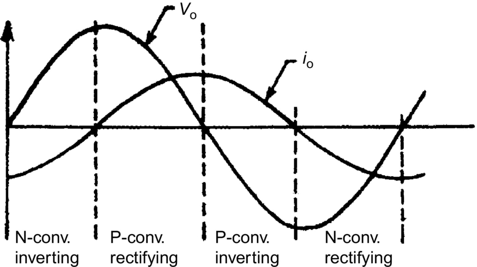
Fig. 14.20A shows the schematic diagram of a three-phase half-wave (three-pulse) cycloconverter feeding a single-phase load and Fig. 14.20B the configuration of a three-phase half-wave (three-pulse) cycloconverter feeding a three-phase load. The basic process of a three-phase cycloconversion is illustrated in Fig. 14.20C at 15 Hz, 0.6 power factor lagging load from a 50 Hz supply. As the firing angle α is cycled from zero at “a” to 180 degrees at “j,” half a cycle of output frequency is produced (the gating circuit is to be suitably designed to introduce this oscillation of the firing angle). For this load, it can be seen that although the mean output voltage reverses at X, the mean output current (assumed sinusoidal) remains positive until Y. During XY, the SCRs A, B, and C in P-converter are “inverting.”

A similar period exists at the end of the negative half cycle of the output voltage when D, E, and F SCRs in N-converter are “inverting.” Thus, the operation of the converter follows in the order of “rectification” and “inversion” in a cyclic manner; the relative durations are dependent on load power factor. The output frequency is that of the firing angle oscillation about a quiescent point of 90 degrees (condition when the mean output voltage, given by ![]() , is zero). For obtaining the positive half cycle of the voltage, firing angle α is varied from 90 to 0 degrees, and then to 90 degrees and, for the negative half cycle, from 90, to 180 degrees, and back to 90 degrees. Variation of α within the limits of 180 degrees automatically provides for “natural” line commutation of the SCRs. It is shown that a complete cycle of low-frequency output voltage is fabricated from the segments of the three-phase input voltage by using the phase-controlled converters. The P-converter or N-converter SCRs receive firing pulses, which are timed such that each converter delivers the same mean output voltage. This is achieved, as in the case of single-phase cycloconverter or the dual converter, by maintaining the firing angle constraints of the two groups as
, is zero). For obtaining the positive half cycle of the voltage, firing angle α is varied from 90 to 0 degrees, and then to 90 degrees and, for the negative half cycle, from 90, to 180 degrees, and back to 90 degrees. Variation of α within the limits of 180 degrees automatically provides for “natural” line commutation of the SCRs. It is shown that a complete cycle of low-frequency output voltage is fabricated from the segments of the three-phase input voltage by using the phase-controlled converters. The P-converter or N-converter SCRs receive firing pulses, which are timed such that each converter delivers the same mean output voltage. This is achieved, as in the case of single-phase cycloconverter or the dual converter, by maintaining the firing angle constraints of the two groups as ![]() . However, the instantaneous voltages of two converters are not identical, and large circulating current may result unless limited by intergroup reactor as shown (circulating current cycloconverter) or completely suppressed by removing the gate pulses from the nonconducting converter by an intergroup blanking logic (circulating current-free cycloconverter).
. However, the instantaneous voltages of two converters are not identical, and large circulating current may result unless limited by intergroup reactor as shown (circulating current cycloconverter) or completely suppressed by removing the gate pulses from the nonconducting converter by an intergroup blanking logic (circulating current-free cycloconverter).
Circulating-Current Mode Operation. Fig. 14.21 shows typical waveforms of a three-pulse cycloconverter operating with circulating current. Each converter conducts continuously with rectifying and inverting modes as shown, and the load is supplied with an average voltage of two converters reducing some of the ripple in the process, the intergroup reactor behaving as a potential divider. The reactor limits the circulating current; the value of its inductance to the flow of load current is one-fourth of its value to the flow of circulating current as the inductance is proportional to the square of the number of turns. The fundamental wave produced by both the converters is the same. The reactor voltage is the instantaneous difference between the converter voltages, and the time integral of this voltage divided by the inductance (assuming negligible circuit resistance) is the circulating current. For a three-pulse cycloconverter, it can be observed that this current reaches its peak when ![]() and
and ![]() .
.

Output Voltage Equation. A simple expression for the fundamental rms output voltage of the cycloconverter and the required variation of the firing angle α can be derived with the following assumptions: (1) the firing angle α in successive half cycles is varied slowly resulting in a low-frequency output, (2) the source impedance and the commutation overlap are neglected, (3) the SCRs are ideal switches, and (4) the current is continuous and ripple-free. The average dc output voltage of a p-pulse dual converter with fixed α is
For the p-pulse dual converter operating as a cycloconverter, the average phase voltage output at any point of the low frequency should vary according to the equation
where Vo1,max is the desired maximum value of the fundamental output of the cycloconverter.
Comparing Eq. (14.25) with Eq. (14.26), the required variation of α to obtain a sinusoidal output is given by
where r is the ratio (Vo1,max/Vdomax), the voltage magnitude control ratio.
Eq. (14.27) shows α as a nonlinear function with ![]() as shown in Fig. 14.22.
as shown in Fig. 14.22.

However, the firing angle αP of the P-converter cannot be reduced to 0 degrees as this corresponds to ![]() for the N-converter, which, in practice, cannot be achieved because of allowance for commutation overlap and finite turn-off time of the SCRs. Thus, the firing angle αP can be reduced to a certain finite value αmin, and the maximum output voltage is reduced by a factor cos αmin.
for the N-converter, which, in practice, cannot be achieved because of allowance for commutation overlap and finite turn-off time of the SCRs. Thus, the firing angle αP can be reduced to a certain finite value αmin, and the maximum output voltage is reduced by a factor cos αmin.
The fundamental rms voltage per phase of either converter is

Though the rms values of the low-frequency output voltage of the P-converter and that of the N-converter are equal, the actual waveforms differ, and the output voltage at the midpoint of the circulating current-limiting reactor (Fig. 14.21), which is the same as the load voltage, is obtained as the mean of the instantaneous output voltages of the two converters.
Circulating Current-free Mode Operation. Fig. 14.23 shows the typical waveforms for a three-pulse cycloconverter operating in this mode with RL load assuming continuous-current operation. Depending on the load current direction, only one converter operates at a time, and the load voltage is the same as the output voltage of the conducting converter. As explained earlier in the case of single-phase cycloconverter, there is a possibility of short circuit of the supply voltages at the crossover points of the converter unless taken care of in the control circuit. The waveforms drawn also neglect the effect of overlap due to the ac supply inductance. A reduction in the output voltage is possible by retarding the firing angle gradually at the points a, b, c, d, and e in Fig. 14.23. (This can be easily implemented by reducing the magnitude of the reference voltage in the control circuit.) The circulating current is completely suppressed by blocking all the SCRs in the converter, which is not delivering the load current. A current sensor is incorporated in each output phase of the cycloconverter, which detects the direction of the output current and feeds an appropriate signal to the control circuit to inhibit or blank the gating pulses to the nonconducting converter in the same way as in the case of a dual converter for dc drives. The circulating current-free operation improves the efficiency and the displacement factor of the cycloconverter and also increases the maximum usable output frequency. The load voltage transfers smoothly from one converter to the other.

14.4.2.2 Three-Phase Six-Pulse and Twelve-Pulse Cycloconverter
A six-pulse cycloconverter circuit configuration is shown in Fig. 14.24. Typical load voltage waveforms for 6-pulse (with 36 SCRs) and 12-pulse (with 72 SCRs) cycloconverters are shown in Fig. 14.25, the 12-pulse converter being obtained by connecting two six-pulse configurations in series and appropriate transformer connections for the required phase shift. It may be seen that the higher pulse numbers will generate waveforms closer to the desired sinusoidal form and thus permit higher frequency output. The phase loads may be isolated from each other as shown or interconnected with suitable secondary winding connections.


14.4.3 Cycloconverter Control Scheme
Various possible control schemes, analog and digital, for deriving trigger signals and for controlling the basic cycloconverter have been developed over the years.
Out of the several possible signal combinations, it has been shown [8] that a sinusoidal reference signal (![]() ) at desired output frequency fo and a cosine modulating signal (
) at desired output frequency fo and a cosine modulating signal (![]() ) at input frequency fi is the best combination possible for comparison to derive the trigger signals for the SCRs (Fig. 14.26 [9]), which produces the output waveform with the lowest total harmonic distortion. The modulating voltages can be obtained as the phase-shifted voltages (B-phase for A-phase SCRs, C-phase voltage for B-phase SCRs, and so on) as explained in Fig. 14.27, where at the intersection point “a”
) at input frequency fi is the best combination possible for comparison to derive the trigger signals for the SCRs (Fig. 14.26 [9]), which produces the output waveform with the lowest total harmonic distortion. The modulating voltages can be obtained as the phase-shifted voltages (B-phase for A-phase SCRs, C-phase voltage for B-phase SCRs, and so on) as explained in Fig. 14.27, where at the intersection point “a”
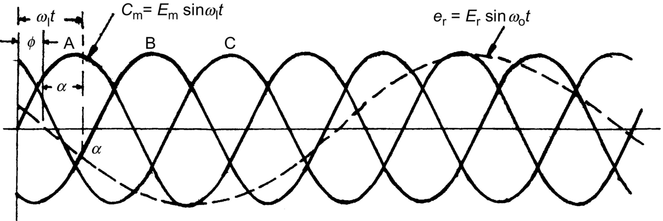
From Fig. 14.27, the firing delay for A-phase SCR, ![]()
The cycloconverter output voltage for continuous-current operation,
in which the equation shows that the amplitude, frequency, and phase of the output voltage can be controlled by controlling corresponding parameters of the reference voltage, thus making the transfer characteristic of the cycloconverter linear. The derivation of the two complimentary voltage waveforms for the P-group or N-group converter “banks” in this way is illustrated in Fig. 14.28. The final cycloconverter output wave shape is composed of alternate half-cycle segments of the complementary P-converter and the N-converter output voltage waveforms that coincide with the positive and negative current half cycles, respectively.

Control Circuit Block Diagram. Fig. 14.29 [10] shows a simplified block diagram of the control circuit for a circulating current-free cycloconverter implemented with ICs in the early seventies in the Power Electronics Laboratory at IIT Kharagpur in India. The same circuit is also applicable to a circulating current cycloconverter with the omission of the converter group selection and blanking circuit.

The synchronizing circuit produces the modulating voltages (![]() ,
, ![]() ,
, ![]() ), synchronized with the mains through step-down transformers and proper filter circuits.
), synchronized with the mains through step-down transformers and proper filter circuits.
The reference source produces variable-magnitude variable-frequency three-phase voltages (era, erb, erc) for comparison with the modulation voltages. Various ways, analog or digital, have been developed to implement this reference source as in the case of the PWM inverter. In one of the early analog schemes, Fig. 14.30 [10], for a three-pulse cycloconverter, a variable-frequency UJT relaxation oscillator of frequency 6fd triggers a ring counter to produce a three-phase square-wave output of frequency fd that is used to modulate a single-phase fixed frequency (fc) variable amplitude sinusoidal voltage in a three-phase full-wave transistor chopper. The three-phase output contains (![]() ), (
), (![]() ), (
), (![]() ), etc. frequency components from where the “wanted” frequency component (
), etc. frequency components from where the “wanted” frequency component (![]() ) is filtered out for each phase using a low-pass filter. For example, with
) is filtered out for each phase using a low-pass filter. For example, with ![]() and frequency of the relaxation oscillator varying between 2820 and 3180 Hz, a three-phase 0–30 Hz reference output can be obtained with the facility for phase sequence reversal.
and frequency of the relaxation oscillator varying between 2820 and 3180 Hz, a three-phase 0–30 Hz reference output can be obtained with the facility for phase sequence reversal.

The logic and trigger circuit for each phase involves comparators for comparison of the reference and modulating voltages and inverters acting as buffer stages. The outputs of the comparators are used to clock the flip-flops or latches whose outputs in turn feed the SCR gates through AND gates and pulse amplifying and isolation circuits; the second input to the AND gates is from the converter group selection and blanking circuit.
In the converter group selection and blanking circuit, the zero crossing of the current at the end of each half cycle is detected and is used to regulate the control signals to either P-group or N-group converters depending on whether the current goes to zero from negative to positive or positive to negative, respectively. However, in practice, the current being discontinuous passes through multiple zero crossings while changing direction, which may lead to undesirable switching of the converters. So, in addition to the current signal, the reference voltage signal is also used for the group selection, and a threshold band is introduced in the current signal detection to avoid inadvertent switching of the converters. Further, a delay circuit provides a blanking period of appropriate duration between the converter groups switching to avoid line-to-line short circuits [10]. In some schemes, the delays are not introduced when a small circulating current is allowed during crossover instants limited by reactors of limited size, and this scheme operates in the so-called “dual mode”—circulating current and circulating current-free mode for minor and major portions of the output cycle, respectively. A different approach to the converter group selection, based on the closed-loop control of the output voltage where a bias voltage is introduced between the voltage transfer characteristics of the converters to reduce circulating current, is discussed in [8].
Improved Control Schemes. With the development of microprocessors and PC-based systems, digital software control has taken over many tasks in modern cycloconverters, particularly in replacing the low-level reference waveform generation and analog signal comparison units. The reference waveforms can be easily generated in the computer, stored in the EPROMs, and accessed under the control of a stored program and microprocessor clock oscillator. The analog signal voltages can be converted to digital signals by using analog-to-digital converters (ADCs). The waveform comparison can then be made with the comparison features of the microprocessor system. The addition of time delays and intergroup blanking can also be achieved with digital techniques and computer software. A modification of the cosine firing control using communication principles, such as regular sampling in preference to the natural sampling (discussed so far) of the reference waveform, yielding a stepped sine wave before comparison with the cosine wave [11] has been shown to reduce the presence of subharmonics (discussed later) in the circulating current cycloconverter and facilitate microprocessor-based implementation, as in the case of PWM inverter.
For a six-pulse noncirculating current cycloconverter-fed synchronous motor drive with a vector control scheme and a flux observer, a PC-based hybrid control scheme (a combination of analog and digital control) has been reported in [12]. Here, the functions such as comparison, group selection, blanking between the groups and triggering signal generation, and filtering and phase conversion are left to the analog controller and digital controller that take care of more serious tasks such as voltage decoupling for current regulation; flux estimation using observer; speed, flux and field current regulators using PI-controllers; and position and speed calculation leading to an improvement of sampling time and design accuracy.
14.4.4 Cycloconverter Harmonics and Input Current Waveform
The exact wave shape of the output voltage of the cycloconverter depends on (1) the pulse number of the converter, (2) the ratio of the output to input frequency (fo/fi), (3) the relative level of the output voltage, (4) the load displacement angle, (5) the circulating current or circulating current-free operation, and (6) the method of control of the firing instants. The harmonic spectrum of a cycloconverter output voltage is different and more complex than that of a phase-controlled converter. It has been revealed [8] that because of the continuous “to-and-fro” phase modulation of the converter firing angles, the harmonic distortion components (known as necessary distortion terms) have frequencies that are sums and differences between multiples of output and input supply frequencies.
Circulating Current-Free Operation. A derived general expression for the output voltage of a cycloconverter with circulating current-free operation [8] shows the following spectrum of harmonic frequencies for the 3-pulse, 6-pulse, and 12-pulse cycloconverters employing cosine modulation technique:
where k is any integer from 1 to infinity and n is any integer from 0 to infinity.
It may be observed that for certain ratios of fo/fi, the order of harmonics may be less or equal to the desired output frequency. All such harmonics are known as subharmonics, since they are not higher multiples of the input frequency. These subharmonics may have considerable amplitudes (e.g., with a 50 Hz input frequency and 35 Hz output frequency, a subharmonic of frequency ![]() is produced whose magnitude is 12.5% of the 35 Hz component [11]) and are difficult to filter and so objectionable. Their spectrum increase with the increase of the ratio fo/fi and so limits its value at which a tolerable waveform can be generated.
is produced whose magnitude is 12.5% of the 35 Hz component [11]) and are difficult to filter and so objectionable. Their spectrum increase with the increase of the ratio fo/fi and so limits its value at which a tolerable waveform can be generated.
Circulating-Current Operation. For circulating current operation with continuous current, the harmonic spectrum in the output voltage is the same as that of the circulating current-free operation except that each harmonic family now terminates at a definite term, rather than having infinite number of components. They are

The amplitude of each harmonic component is a function of the output voltage ratio for the circulating current cycloconverter and the output voltage ratio and the load displacement angle for the circulating current-free mode.
From the point of view of maximum useful attainable output-to-input frequency ratio (fi/fo) with the minimum amplitude of objectionable harmonic components, a guideline is available in [8] for it as 0.33, 0.5, and 0.75 for 3-, 6-, and 12-pulse cycloconverter, respectively. However, with the modification of the cosine-wave modulation timings like regular sampling [11] in the case of circulating current cycloconverters only and using a subharmonic detection and feedback control concept [13,14] for both circulating and circulating current-free cases, the subharmonics can be suppressed, and useful frequency range for the naturally commutated cycloconverters can be increased.
Other Harmonic Distortion Terms. Besides the harmonics as mentioned, other harmonic distortion terms consisting of frequencies of integral multiples of desired output frequency appear if the transfer characteristic between the output and reference voltages is not linear. These are called unnecessary distortion terms that are absent when the output frequencies are much less than the input frequency. Further, some practical distortion terms may appear due to some practical nonlinearities and imperfections in the control circuits of the cycloconverter, particularly at relatively lower levels of output voltage.
Input Current Waveform. Although the load current, particularly for higher pulse cycloconverters can be assumed to be sinusoidal, the input current is more complex being made of pulses. Assuming the cycloconverter to be an ideal switching circuit without losses, it can be shown from the instantaneous power balance equation that in cycloconverter supplying a single-phase load, the input current has harmonic components of frequencies ![]() called characteristic harmonic frequencies that are independent of pulse number, and they result in an oscillatory power transmittal to the ac supply system. In the case of cycloconverter feeding a balanced three-phase load, the net instantaneous power is the sum of the three oscillating instantaneous powers when the resultant power is constant, and the net harmonic component is much reduced compared with that of a single-phase load case. In general, the total rms value of the input current waveform consists of three components: in-phase, quadrature, and the harmonic. The in-phase component depends on the active power output, while the quadrature component depends on the net average of the oscillatory firing angle and is always lagging.
called characteristic harmonic frequencies that are independent of pulse number, and they result in an oscillatory power transmittal to the ac supply system. In the case of cycloconverter feeding a balanced three-phase load, the net instantaneous power is the sum of the three oscillating instantaneous powers when the resultant power is constant, and the net harmonic component is much reduced compared with that of a single-phase load case. In general, the total rms value of the input current waveform consists of three components: in-phase, quadrature, and the harmonic. The in-phase component depends on the active power output, while the quadrature component depends on the net average of the oscillatory firing angle and is always lagging.
14.4.5 Cycloconverter Input Displacement/Power Factor
The input supply performance of a cycloconverter such as displacement factor or fundamental power factor, input power factor, and the input current distortion factor is defined similar to those of the phase-controlled converter. The harmonic factor for the case of a cycloconverter is relatively complex as the harmonic frequencies are not simple multiples of the input frequency but are sums and differences between multiples of output and input frequencies.
Irrespective of the nature of the load, leading, lagging, or unity power factor, the cycloconverter requires reactive power decided by the average firing angle. At low-output voltage, the average phase displacement between the input current and the voltage is large, and the cycloconverter has a low input displacement and power factor. Besides load displacement factor and output voltage ratio, another component of the reactive current arises due to the modulation of the firing angle in the fabrication process of the output voltage [8]. In a phase-controlled converter supplying dc load, the maximum displacement factor is unity for maximum dc output voltage. However, in the case of the cycloconverter, the maximum input displacement factor is 0.843 with unity power factor load [8,15]. The displacement factor decreases with reduction in the output voltage ratio. The distortion factor of the input current is given by (I1/I), which is always less than 1, and the resultant power factor (= distortion factor × displacement factor) is thus much lower (around 0.76 maximum) than the displacement factor, and this is a serious disadvantage of the naturally commutated cycloconverter (NCC).
14.4.6 Effect of Source Impedance
The source inductance introduces commutation overlap and affects the external characteristics of a cycloconverter similar to the case of a phase-controlled converter with the dc output. It introduces delay in transfer of current from one SCR to another and results in a voltage loss at the output and a modified harmonic distortion. At the input, the source impedance causes “rounding off” of the steep edges of the input current waveforms, resulting in reduction in the amplitudes of higher order harmonic terms and a decrease in the input displacement factor.
14.4.7 Simulation Analysis of Cycloconverter Performance
The nonlinearity and discrete time nature of practical cycloconverter systems, particularly for discontinuous-current conditions, make an exact analysis quite complex, and a valuable design and analytic tool is a digital computer simulation of the system. Two general methods of computer simulation of the cycloconverter waveforms for RL and induction motor loads with circulating current and circulating current-free operation have been suggested in [16] where one of the methods that is very fast and convenient is the crossover point method that gives the crossover points (intersections of the modulating and reference waveforms) and the conducting phase numbers for both P- and N-converters from which the output waveforms for a particular load can be digitally computed at any interval of time for a practical cycloconverter.
14.4.8 Power Quality Issues
Degradation of power quality (PQ) in a cycloconverter-fed system due to subharmonics/interharmonics in the input and the output has been a subject of recent studies [14,17]. In [17], the study includes the impact of cycloconverter control strategies on the total harmonic distortion (THD), distribution transformers, and communication lines, while in [14], the PQ indices are suitably defined and the effect on THD, input/output displacement factor, and input/output power factor for a cycloconverter-fed synchronous motor drive is studied together with a development of a simple feedback method of reduction of subharmonics/low-frequency interharmonics for the improvement of the power quality. The implementation of this scheme, detailed in [14], requires a simple modification of the control circuit of the cycloconverter in contrast to the expensive power level active filters otherwise required for suppression of such harmonics [18].
14.4.9 Forced Commutated Cycloconverter
The naturally commutated cycloconverter (NCC) with SCRs as devices, so far discussed, is sometimes referred to as a restricted frequency changer; in view of the allowance on the output voltage quality ratings, the maximum output voltage frequency is restricted (![]() ), as mentioned earlier. With devices replaced by fully controlled switches like forced commutated SCRs, power transistors, IGBTs, and GTOs, a forced commutated cycloconverter can be built where the desired output frequency is given by
), as mentioned earlier. With devices replaced by fully controlled switches like forced commutated SCRs, power transistors, IGBTs, and GTOs, a forced commutated cycloconverter can be built where the desired output frequency is given by ![]() , where fs is the switching frequency, which may be larger or smaller than the fi. In the case when
, where fs is the switching frequency, which may be larger or smaller than the fi. In the case when ![]() , the converter is called unrestricted frequency changer (UFC) and when
, the converter is called unrestricted frequency changer (UFC) and when ![]() , it is called a slow switching frequency changer (SSFC). The early FCC structures have been comprehensively treated in [15]. It has been shown that in contrast with the NCC, where the input displacement factor (IDF) is always lagging, in UFC, it is leading when the load displacement factor is lagging and vice versa, and in SSFC, it is identical to that of the load. Further, with proper control in an FCC, the input displacement factor can be made unity displacement factor frequency changer (UDFFC) with concurrent composite voltage waveform or controllable displacement factor frequency changer (CDFFC), where P-converter and N-converter voltage segments can be shifted relative to the output current wave for control of IDF continuously from lagging via unity to leading.
, it is called a slow switching frequency changer (SSFC). The early FCC structures have been comprehensively treated in [15]. It has been shown that in contrast with the NCC, where the input displacement factor (IDF) is always lagging, in UFC, it is leading when the load displacement factor is lagging and vice versa, and in SSFC, it is identical to that of the load. Further, with proper control in an FCC, the input displacement factor can be made unity displacement factor frequency changer (UDFFC) with concurrent composite voltage waveform or controllable displacement factor frequency changer (CDFFC), where P-converter and N-converter voltage segments can be shifted relative to the output current wave for control of IDF continuously from lagging via unity to leading.
In addition to allowing bilateral power flow, UFCs offer an unlimited output frequency range, offer good input voltage utilization, do not generate input current and output voltage subharmonics, and require only nine bidirectional switches (Fig. 14.31) for a three-phase to three-phase conversion. The main disadvantage of the structures treated in [15] is that they generate large unwanted low-order input current and output voltage harmonics that are difficult to filter out, particularly for low-output voltage conditions. This problem has largely been solved with an introduction of an imaginative PWM voltage control scheme in [19], which is the basis of the newly designated converter called the matrix converter (also known as PWM cycloconverter) that operates as a generalized solid-state transformer with significant improvement in voltage and input current waveforms resulting in sine-wave input and sine-wave output as discussed in the next section.
 matrix converter circuit with input filter and clamp circuit; bidirectional switch configuration as (B) common emitter, (C) common collector, (D) transistor-diode bridge configuration, and (E) reverse blocking IGBT (RB-IGBT); and (F) switching matrix symbol for converter in (A).
14.5 Matrix Converter
The matrix converter (MC) is a development of the FCC that employs bidirectional fully controlled switches, incorporating PWM voltage control, as mentioned earlier. With the initial progress made by Venturini [19–21], it has received considerable attention in recent years as it provides a good alternative to the conventionally employed rectifier-inverter topology or the back-to-back topology, having the advantages of being a single-stage converter with only nine switches for three-phase to three-phase conversion and inherent bidirectional power flow, sinusoidal input/output waveforms with moderate switching frequency, possibility of a compact design due to the absence of bulky dc link reactive components, and controllable input power factor independent of the output load current. Along with these theoretical advantages, [22] has mentioned advantages of MCs over conventional dc link variant as exhibition of better operation under high-temperature conditions, less voltage stress per switch, and less maintenance. The main disadvantages of the matrix converters developed so far are the inherent restriction of the voltage transfer ratio (0.866); more complex control, commutation, and protection strategy; and, above all, commercial nonavailability of a fully controlled bidirectional high frequency switch integrated in a silicon chip.
The power circuit diagram of the most practical three-phase to three-phase (![]() ) matrix converter is shown in Fig. 14.31A, which uses nine bidirectional switches so arranged that any of the three-input phases can be connected to any output phase as is shown symbolically in the switching matrix in Fig. 14.31F. The circuit is called a matrix converter as it provides exactly one switch for each of the possible connections between the input and the output. The voltage at any input terminal may be made to appear at any output terminal or terminals, while the current in any phase of the load may be drawn from any phase or phases of the input supply under following restrictions:
) matrix converter is shown in Fig. 14.31A, which uses nine bidirectional switches so arranged that any of the three-input phases can be connected to any output phase as is shown symbolically in the switching matrix in Fig. 14.31F. The circuit is called a matrix converter as it provides exactly one switch for each of the possible connections between the input and the output. The voltage at any input terminal may be made to appear at any output terminal or terminals, while the current in any phase of the load may be drawn from any phase or phases of the input supply under following restrictions:
(a) Only one switch of the output leg can be closed due to the presence of capacitors.
(b) At least one switch in the output leg must be closed, as the inductive nature of the load makes it impossible to interrupt the load current suddenly.
Thus, one and only one switch in the output leg is to be closed. With these constraints, it can be visualized that out of the possible 512 ![]() states of the converter, only 27 switch combinations are allowed as given in Table 14.1, which includes the resulting output line voltages and input phase currents. These combinations are divided into three groups. Group I consists of six combinations when each output phase is connected to a different input phase. In group II, there are three subgroups each having six combinations with two-output phases short-circuited (connected to the same input phase). Group III includes three combinations with all output phases short-circuited. For the switches, the inverse-parallel combination of reverse blocking self-controlled devices like power MOSFETs or IGBTs or transistor-embedded diode bridge as shown in Fig 14.3B–E has been used so far. Fig. 14.31B and C are the conventionally employed common emitter and common collector configurations, respectively. These configurations allow soft switching from one bidirectional switch to other. The latter has an advantage that it requires less number of insulated power supplies to drive the switches than the former configuration [23]. New perspective configuration of the bidirectional switch is to use two RB-IGBTs with reverse blocking capability in antiparallel (symbol of which is shown in Fig 14.31E). This configuration leads to elimination of external diodes, which results in reduction in conduction losses and the transistor size [24].
states of the converter, only 27 switch combinations are allowed as given in Table 14.1, which includes the resulting output line voltages and input phase currents. These combinations are divided into three groups. Group I consists of six combinations when each output phase is connected to a different input phase. In group II, there are three subgroups each having six combinations with two-output phases short-circuited (connected to the same input phase). Group III includes three combinations with all output phases short-circuited. For the switches, the inverse-parallel combination of reverse blocking self-controlled devices like power MOSFETs or IGBTs or transistor-embedded diode bridge as shown in Fig 14.3B–E has been used so far. Fig. 14.31B and C are the conventionally employed common emitter and common collector configurations, respectively. These configurations allow soft switching from one bidirectional switch to other. The latter has an advantage that it requires less number of insulated power supplies to drive the switches than the former configuration [23]. New perspective configuration of the bidirectional switch is to use two RB-IGBTs with reverse blocking capability in antiparallel (symbol of which is shown in Fig 14.31E). This configuration leads to elimination of external diodes, which results in reduction in conduction losses and the transistor size [24].
Table 14.1
Three-phase/three-phase matrix converter switching combinations
| Group | a | b | c | vab | vbc | vca | iA | iB | iC | SAa | SAb | SAc | SBa | SBb | SBc | SCa | SCb | SCc |
| I | A | B | C | vAB | vBC | vCA | ia | ib | ic | 1 | 0 | 0 | 0 | 1 | 0 | 0 | 0 | 1 |
| A | C | B | ia | ic | ib | 1 | 0 | 0 | 0 | 0 | 1 | 0 | 1 | 0 | ||||
| B | A | C | ib | ia | ic | 0 | 1 | 0 | 1 | 0 | 0 | 0 | 0 | 1 | ||||
| B | C | A | vBC | vCA | vAB | ic | ia | ib | 0 | 1 | 0 | 0 | 0 | 1 | 0 | 1 | 0 | |
| C | A | B | vCA | vAB | vBC | ib | ic | ia | 0 | 0 | 1 | 1 | 0 | 0 | 0 | 1 | 0 | |
| C | B | A | ic | ib | ia | 0 | 0 | 1 | 0 | 1 | 0 | 1 | 0 | 0 | ||||
| II-A | A | C | C | 0 | vCA | ia | 0 | 1 | 0 | 0 | 0 | 0 | 1 | 0 | 0 | 1 | ||
| B | C | C | vBC | 0 | 0 | ia | 0 | 1 | 0 | 0 | 0 | 1 | 0 | 0 | 1 | |||
| B | A | A | 0 | ia | 0 | 0 | 1 | 0 | 1 | 0 | 0 | 1 | 0 | 0 | ||||
| C | A | A | vCA | 0 | 0 | ia | 0 | 0 | 1 | 1 | 0 | 0 | 1 | 0 | 0 | |||
| C | B | B | 0 | vBC | 0 | ia | 0 | 0 | 1 | 0 | 1 | 0 | 0 | 1 | 0 | |||
| A | B | B | vAB | 0 | ia | 0 | 1 | 0 | 0 | 0 | 1 | 0 | 0 | 1 | 0 | |||
| II-B | C | A | C | 0 | ib | 0 | 0 | 0 | 1 | 1 | 0 | 0 | 0 | 0 | 1 | |||
| C | B | C | vBC | 0 | 0 | ib | 0 | 0 | 1 | 0 | 1 | 0 | 0 | 0 | 1 | |||
| A | B | A | vAB | 0 | ib | 0 | 1 | 0 | 0 | 0 | 1 | 0 | 1 | 0 | 0 | |||
| A | C | A | vCA | 0 | 0 | ib | 1 | 0 | 0 | 0 | 0 | 1 | 1 | 0 | 0 | |||
| B | C | B | vBC | 0 | 0 | ib | 0 | 1 | 0 | 0 | 0 | 1 | 0 | 1 | 0 | |||
| B | A | B | vAB | 0 | ib | 0 | 0 | 1 | 0 | 1 | 0 | 0 | 0 | 1 | 0 | |||
| II-C | C | C | A | 0 | vCA | ic | 0 | 0 | 0 | 1 | 0 | 0 | 1 | 1 | 0 | 0 | ||
| C | C | B | 0 | vBC | 0 | ic | 0 | 0 | 1 | 0 | 0 | 1 | 0 | 1 | 0 | |||
| A | A | B | 0 | vAB | ic | 0 | 1 | 0 | 0 | 1 | 0 | 0 | 0 | 1 | 0 | |||
| A | A | C | 0 | vCA | 0 | ic | 1 | 0 | 0 | 1 | 0 | 0 | 0 | 0 | 1 | |||
| B | B | C | 0 | vBC | 0 | ic | 0 | 1 | 0 | 0 | 1 | 0 | 0 | 0 | 1 | |||
| B | B | A | 0 | vAB | ic | 0 | 0 | 1 | 0 | 0 | 1 | 0 | 1 | 0 | 0 | |||
| III | A | A | A | 0 | 0 | 0 | 0 | 0 | 0 | 0 | 0 | 0 | 1 | 0 | 0 | 1 | 0 | 0 |
| B | B | B | 0 | 0 | 0 | 0 | 0 | 0 | 0 | 0 | 0 | 0 | 1 | 0 | 0 | 1 | 0 | |
| C | C | C | 0 | 0 | 0 | 0 | 0 | 0 | 0 | 0 | 0 | 0 | 0 | 1 | 0 | 0 | 1 |

With a given set of input three-phase voltages, any desired set of three-phase output voltages can be synthesized by adopting a suitable switching strategy. However, it has been shown [21,25,26] that regardless of the switching strategy, there are physical limits on the achievable output voltage with these converters as the maximum peak-to-peak output voltage cannot be greater than the minimum voltage difference between two phases of the input. To have complete control of the synthesized output voltage, the envelope of the three-phase reference or target voltages must be fully contained within the continuous envelope of the three-phase input voltages. Initial strategy with the output frequency voltages as references reported the limit as 0.5 of the input as shown in Fig. 14.32A. This can be increased to 0.866 by adding a third harmonic voltage of input frequency (Vi/4)cos3ωit to all target output voltages and subtracting from them a third harmonic voltage of output frequency (Vo/6)cos3ωot as shown in Fig. 14.32B [21,25]. The increase in amplitude is shown through line voltages (vab) in Fig. 14.32C. In fact, it is shown in [26] that the above optimization can be extended to m×n matrix converter (where m and n are both odd) by adding mth and subtracting the nth harmonic from all the target output voltages. Details on multiphase matrix converters are given in Chapter 16. However, this process involves considerable amount of additional computations in synthesizing the output voltages. The other alternative is to use the space vector modulation (SVM) strategy as used in PWM inverters without adding third harmonic components, but it also yields the maximum voltage transfer ratio as 0.866.

An ac input LC filter is used to eliminate the switching ripples generated in the converter, and the load is assumed to be sufficiently inductive to maintain continuity of the output currents. Work on input side filters can be seen in [27–29].
14.5.1 Operation and Control of Matrix Converter
The converter in Fig. 14.31 connects any input phase (A, B, and C) to any output phase (a, b, and c) at any instant. When connected, the voltages van, vbn, and vcn at the output terminals are related to the input voltages VAo, VBo, and VCo as
where SAa through SCc are the switching variables of the corresponding switches shown in Fig. 14.31. For a balanced linear star-connected load at the output terminals, the input phase currents are related to the output phase currents by

Note that the matrix of the switching variables in Eq. (14.33) is a transpose of the respective matrix in Eq. (14.32). The matrix converter should be controlled using a specific and appropriately timed sequence of the values of the switching variables, which will result in balanced output voltages having the desired frequency and amplitude, while the input currents are balanced and in phase (for unity IDF) or at an arbitrary angle (for controllable IDF) with respect to the input voltages. As the matrix converter, in theory, can operate at any frequency and at the output or input, including zero, it can be employed as a three-phase ac-dc converter, dc/three-phase ac converter, or even a buck/boost dc chopper and thus as a universal power converter.
The control methods adopted so far for the matrix converter are quite complex and are subjects of continuing research [21–39]. Out of several methods proposed for independent control of the output voltages and input currents, two methods are of wide use and will be briefly reviewed here: (1) the Venturini method based on a mathematical approach of transfer function analysis and (2) the space vector modulation (SVM) approach (as has been standardized now in the case of PWM control of the dc link inverter).
Venturini Method. Given a set of three-phase input voltages with constant amplitude Vi and frequency ![]() , this method calculates a switching function involving the duty cycles of each of the nine bidirectional switches and generates the three-phase output voltages by sequential piecewise sampling of the input waveforms. These output voltages follow a predetermined set of reference or target voltage waveforms and with a three-phase load connected, a set of input currents Ii and angular frequency ωi should be in phase for unity IDF or at a specific angle for controlled IDF.
, this method calculates a switching function involving the duty cycles of each of the nine bidirectional switches and generates the three-phase output voltages by sequential piecewise sampling of the input waveforms. These output voltages follow a predetermined set of reference or target voltage waveforms and with a three-phase load connected, a set of input currents Ii and angular frequency ωi should be in phase for unity IDF or at a specific angle for controlled IDF.
A transfer function approach is used in [36] to achieve the abovementioned features by relating the input and output voltages and the output and input currents as


where the elements of the modulation matrix, mij(t), (![]() ) represent the duty cycles of a switch connecting output phase i to input phase j within a sample switching interval. The elements of mij(t) are limited by the constraints discussed above and are mathematically written as
) represent the duty cycles of a switch connecting output phase i to input phase j within a sample switching interval. The elements of mij(t) are limited by the constraints discussed above and are mathematically written as
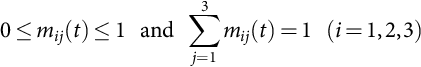
The set of three-phase target or reference voltages to achieve the maximum voltage transfer ratio for unity IDF is

where Vom and Vim are the magnitudes of output and input fundamental voltages of angular frequencies ωo and ωi, respectively. With ![]() , a general formula for the duty cycles mij(t) is derived in [36]. For unity IDF condition, a simplified formula is
, a general formula for the duty cycles mij(t) is derived in [36]. For unity IDF condition, a simplified formula is

where ![]() and
and ![]() .
.
The method developed as above is based on a direct transfer function (DTF) approach using a single modulation matrix for the matrix converter, employing the switching combinations of all the three groups in Table 14.1. Another approach called indirect transfer function (ITF) approach [30,31] considers the matrix converter as a combination of PWM voltage source rectifier-PWM voltage source inverter (VSR-VSI) and employs the already well-established VSR and VSI PWM techniques for MC control utilizing the switching combinations of group II and group III only of Table 14.1. The drawback of this approach is that the IDF is limited to unity, and the method also generates higher and fractional harmonic components in the input and the output waveforms. This method can also be found in [40].
A simplified direct transfer function approach at unity IDF can be developed. Eq. (14.34) and the constraint equations can be rewritten as follows:

X is the modulation vector, and the elements can be derived as
AAT when solved will have terms ![]() and
and ![]() , so, let
, so, let ![]() and
and ![]() . Each term of X, when (14.39) is solved, is of similar pattern and can be shown as
. Each term of X, when (14.39) is solved, is of similar pattern and can be shown as
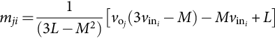
where Mji is the time-based index corresponding to the switch Sji that connects j-th output to the i-th input. The time duration for which this switch is on, is calculated by multiplying this index with sampling time. Further solving by considering m balanced input phases, and finally neglecting the terms with denominators with high value, solution for m×n matrix converter is written as
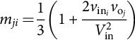
A detailed simulation with this modulation scheme can be seen in [41].
SVM Method. The space vector modulation is a well-documented inverter PWM control technique that yields high-voltage gain and less harmonic distortion compared with the other modulation techniques. Here, the three-phase input currents and output voltages are represented as space vectors, and SVM is simultaneously applied to the output voltage and input current space vectors, while the matrix converter is modeled as a rectifying and inverting stage by the indirect modulation method (Fig. 14.33). Applications of SVM algorithm to control of matrix converters have appeared extensively in the literature [33–38,42–47] and shown to have inherent capability to achieve full control of the instantaneous output voltage vector and the instantaneous current displacement angle even under supply voltage disturbances. The algorithm is based on the concept that the MC output line voltages for each switching combination can be represented as a voltage space vector defined by

Out of the three groups in Table 14.1, only the switching combinations of group II and group III are employed for the SVM method. Group II consists of switching state voltage vectors having constant angular positions and are called active or stationary vectors. Each subgroup of group II determines the position of the resulting output voltage space vector and the six-state space voltage vectors form a six-sextant hexagon used to synthesize the desired output voltage vector. Group III comprises the zero vectors positioned at the center of the output voltage hexagon, and these are suitably combined with the active vectors for the output voltage synthesis.
The modulation method involves selection of the vectors and their on-time computation. At each sampling period Ts, the algorithm selects four active vectors related to any possible combinations of output voltage and input current sectors in addition to the zero vector to construct a desired reference voltage. The amplitude and the phase angle of the reference voltage vector are calculated, and the desired phase angle of the input current vector is determined in advance. For computation of the on-time periods of the chosen vectors, these are combined into two sets leading to two new vectors adjacent to the reference voltage vector in the sextant and having the same direction as the reference voltage vector. Applying the standard SVM theory, the general formulas derived for the vector on-times that satisfy, at the same time, the reference output voltage and input current displacement angle in [36] are

where q is voltage transfer ratio, ϕi is the input displacement angle chosen to achieve the desired input power factor (with ![]() , a maximum value of
, a maximum value of ![]() is obtained), and θo and θi are the phase displacement angles of the output voltage and input current vectors, respectively, whose values are limited within the 0–60degrees range. The on-time of the zero vector is
is obtained), and θo and θi are the phase displacement angles of the output voltage and input current vectors, respectively, whose values are limited within the 0–60degrees range. The on-time of the zero vector is
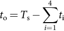
The integral value of the reference vector is calculated over one sample time interval as the sum of the products of the two adjacent vectors and their on-time ratios, and the process is repeated at every sample instant.
Control Implementation and Comparison of the Two Methods. Both the methods need a digital signal processor (DSP)-based system for their implementation. In one scheme [36] for the Venturini method, the programmable timers, as available, are used to time out the PWM gating signals. The processor calculates the six-switch duty cycles in each sampling interval, converts them to integer counts, and stores them in the memory for the next sampling period. In the SVM method, an erasable programmable read-only memory (EPROM) is used to store the selected sets of active and zero vectors, and the DSP calculates the on-times of the vectors. Then, with an identical procedure as in the other method, the timers are loaded with the vector on-times to generate PWM waveforms through suitable output ports. The total computation time of the DSP for the SVM method has been found to be much less than that of the Venturini method. Comparison of the two schemes shows that while in the SVM method the switching losses are lower, the Venturini method shows better performance in terms of input current and output voltage harmonics.
A direct control method as used in conjunction with the voltage source converters has been developed recently and implemented with a 10 kVA matrix converter [48]. Moreover, the voltage transfer ratio can be increased by going into overmodulation. Enhanced methods employing SVM are discussed in [49,50] in which VTR of 0.92 is achieved.
14.5.2 Commutation and Protection Issues in a Matrix Converter
As the matrix converter has no dc link energy storage, any disturbance in the input supply voltage will affect the output voltage immediately, and a proper protection mechanism has to be incorporated, particularly against overvoltage from the supply and overcurrent in the load side. As mentioned, two types of bidirectional switch configurations have hitherto been used: one, the transistor (now IGBT) embedded in a diode bridge and, the other, the two IGBTs in antiparallel with reverse voltage blocking diodes (shown in Fig. 14.31B and C). In the latter configuration, each diode and IGBT combination operates in two quadrants only, which eliminates the circulating currents otherwise built up in the diode bridge configuration that can be limited by only bulky commutation inductors in the lines.
Commutation. The MC does not contain freewheeling diodes that usually achieve safe commutation in the case of other converters. To maintain the continuity of the output current as each switch turns off, the next switch in sequence must be immediately turned on. In practice, with bidirectional switches, a momentary short circuit may develop between the input phases when the switches cross over, and one solution for the configurations shown in Fig. 14.31B, C, and E is to use a semisoft current commutation using a multistepped switching procedure to ensure safe commutation [51–53]. This method requires independent control of each two-quadrant switches, sensing the direction of the load current and introducing a delay during the change of switching states. The switching rule for proper commutation from S1 to S2 of the arrangement shown in Fig. 14.34 for ![]() with the two-quadrant switches for four-stepped commutation [51,53] is (a) turn off S1B, (b) turn on S2A, (c) turn off S1A, and (d) turn on S2B.
with the two-quadrant switches for four-stepped commutation [51,53] is (a) turn off S1B, (b) turn on S2A, (c) turn off S1A, and (d) turn on S2B.

Analogously, for ![]() , the switching rule will be (a) turn off S1A, (b) turn on S2B, (c) turn off S1B, and (d) turn on S2A. These steps for both the cases are shown diagrammatically in Fig. 14.35.
, the switching rule will be (a) turn off S1A, (b) turn on S2B, (c) turn off S1B, and (d) turn on S2A. These steps for both the cases are shown diagrammatically in Fig. 14.35.

Typically, these commutation strategies are now implemented using programmable logic devices such as field-programmable gate array (FPGA) and programmable logic device (PLD) [53,54]. Also, it is worth mentioning that the configuration shown in Fig 14.31D has to stick to two-step commutation that despite of having a considerable advantage of employing less number of switches will produce more spikes in the output voltages.
A robust voltage commutation scheme without sacrificing the line side current waveform quality and with minimal information requirement has been reported recently [55]. Another way to achieve better commutation is by Z-sourcing the input of the matrix converter [56].
Protection Strategies. A clamp capacitor (typically 2 μF for a 3 kW permanent magnet (PM) motor) connected through two three-phase full-bridge diode rectifiers involving additional 12 diodes as shown in Fig. 14.31A (a new configuration has been reported in [57] where the number of additional diodes is reduced to six using the antiparallel switch diodes at the input and output lines of the MC) serves as a voltage clamp for possible voltage spikes under normal and fault conditions. A new passive protection strategy involving suppressor diodes and varistors for excellent overvoltage protection is discussed recently in [58], which allows the removal of the large and expensive diode clamp. A snubberless solution for overvoltage protection is presented in [59].
Input Filter. A three-phase single-stage LC filter at the input consisting of three capacitors in star and three inductors in the line is used to adequately attenuate the higher order harmonics and render sinusoidal input current. Typical values of L and C based on a 415 V converter with a maximum line current of 6.5 A and a switching frequency of 20 kHz are 3 mH and 1.5 μF only [60]. The filter may cause minor phase shift in the input displacement angle that needs correction. Another filter designs can be seen in [28,29]. Ref. [61] lately has employed the input filter capacitors as an energy exchange devices to enhance the ride-through capability of the matrix converter. Ref. [62] discusses the designing of an EMI filter for matrix converter applications.
Fig. 14.36 shows typical experimental waveforms of output line voltage and line current of an MC. The output line current is mostly sinusoidal except a small ripple, when the switching frequency is around 1 kHz only.

14.5.3 Multilevel Matrix converter
Erickson and Al-Naseem [63] introduced a multilevel matrix converter with four-quadrant dc link H-bridge switching cells as shown in Fig 14.37 in 2001. These are suitable for medium- or high-voltage ac-to-ac power conversion. The use of four transistors in the switch cell of Fig. 14.37A allows the average current to be doubled, relative to the conventional matrix converter whose four-quadrant switches are realized using two transistors and two diodes. With dc capacitor, the switch cell is capable of producing instantaneous voltages ![]() , 0,
, 0, ![]() . These converters can both increase and decrease the voltage amplitude with arbitrary power factors. With series connection of switch cells in each branch of the matrix, multilevel switching can be attained with device voltages locally clamped to dc capacitor voltages. Several types of multilevel matrix converter topologies have been proposed over the years, including a novel capacitor-clamped one and with a space vector modulation [64,65]. In [65], the converter utilizes flying capacitors to balance voltage distribution of series-connected bidirectional switches and provide middle-voltage levels.
. These converters can both increase and decrease the voltage amplitude with arbitrary power factors. With series connection of switch cells in each branch of the matrix, multilevel switching can be attained with device voltages locally clamped to dc capacitor voltages. Several types of multilevel matrix converter topologies have been proposed over the years, including a novel capacitor-clamped one and with a space vector modulation [64,65]. In [65], the converter utilizes flying capacitors to balance voltage distribution of series-connected bidirectional switches and provide middle-voltage levels.
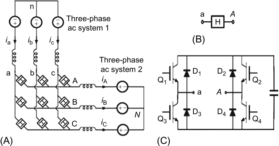
Recently, with cascaded combination of multiple matrix converter (MC) modules, principles of high-power multimodular matrix converters (MMMCs) built from three-input two-output matrix converter (![]() MC) have been presented in [66] with modulation schemes to synthesize sinusoidal waveforms on both sides of the converters. Recent work on modulation strategies on MMMCs can be seen in [67–69]. The circuit shown in Fig. 14.38 is known as MMMC-I. Another structure is discussed in these papers in which nine modules of 3×2 MCs are employed. This is an extension of the first topology and attains a multilevel structure for higher power output and better line side harmonic performance. These topologies feature modular design and bidirectional power flow and enable the use of low-voltage power devices. They may serve as potential candidates for high-power applications where regenerative capability and power density are of importance. However, the drawbacks of them are large number of devices and the use of the input transformer.
MC) have been presented in [66] with modulation schemes to synthesize sinusoidal waveforms on both sides of the converters. Recent work on modulation strategies on MMMCs can be seen in [67–69]. The circuit shown in Fig. 14.38 is known as MMMC-I. Another structure is discussed in these papers in which nine modules of 3×2 MCs are employed. This is an extension of the first topology and attains a multilevel structure for higher power output and better line side harmonic performance. These topologies feature modular design and bidirectional power flow and enable the use of low-voltage power devices. They may serve as potential candidates for high-power applications where regenerative capability and power density are of importance. However, the drawbacks of them are large number of devices and the use of the input transformer.

14.5.4 Indirect Matrix Converters
A conventional matrix converter (CMC) as shown in Fig. 14.31A requires nine bidirectional switches, usually constructed using 18 IGBTs, to switch the three-input phases between the three-output phases. The indirect matrix converters (IMCs), as seen in Fig. 14.40A also have 18 controllable switches. The difference lies in the control of such a converter. This configuration is easier to implement as the control strategies of controlled rectifiers, and inverters can be directly implemented. This topology was first introduced in [70] and later discussed in [71]. It employs 18 controllable switches out 12 are used in rectification and 6 in inversion process. The sparse matrix converter (SMC) (Fig. 14.39) is derived from the IMC that is split into an input stage and output stage without any capacitance in the dc link. The input stage is arranged so that only nine switches are required, while the output stage has a standard six-switch configuration. Thus, the SMC has a total of 15 switches compared with 18 for a CMC and IMC. The functional equivalence, the controllability, and the operating range of the SMC are the same as CMC despite the reduced number of unipolar turn-off power switches [72]. Further reduction of the number of IGBTs is possible with ultra sparse matrix converter (USMC) [73], Fig. 14.40 having 12 IGBTs, with restricted operation to a unidirectional power flow and controllability of the phase displacement of input voltage and current fundamental to ![]() [73]. Very recently, a space vector modulation scheme for an indirect three-level sparse matrix converter (I3 SMC), which is a combination of a three-level neutral-clamped voltage source inverter and an indirect matrix converter, has been discussed in [74]. A 100 kHz SiC sparse matrix converter using 1300 V and 4 A SiC JFET cascade devices has been reported in [75], which is suitable for aircraft applications where a low-volume/low-weight converter is desired. Ref. [76] also introduced a topology with 12 switches employing unidirectional switches in the rectification process. Real-time implementation of an IMC employing SVM algorithms can be seen in [77].
[73]. Very recently, a space vector modulation scheme for an indirect three-level sparse matrix converter (I3 SMC), which is a combination of a three-level neutral-clamped voltage source inverter and an indirect matrix converter, has been discussed in [74]. A 100 kHz SiC sparse matrix converter using 1300 V and 4 A SiC JFET cascade devices has been reported in [75], which is suitable for aircraft applications where a low-volume/low-weight converter is desired. Ref. [76] also introduced a topology with 12 switches employing unidirectional switches in the rectification process. Real-time implementation of an IMC employing SVM algorithms can be seen in [77].


14.5.5 Single-Phase Matrix Converters
The first single-phase matrix converter was studied by Zuckerberger in [78]. In this paper, converter operation was shown to step down the voltage and step up the frequency. Later in [79], step-up/down frequency operation with safe commutation strategy was developed. The limitation of above schemes lied in boosting of output voltages beyond input voltage. This was overcome by introducing single-phase Z-source matrix converter by Nguyen et al. shown in Fig. 14.41, and step-up/step-down of both voltage and frequency was achieved [80]. A family of high-frequency isolated single-phase Z-source matrix converter with safe commutation strategy is discussed in [81]. Another single-phase matrix converter can be seen in [82–86]. An ac Z-source converter based on gamma structure with safe commutation is discussed in [87]. A novel T-type single-phase ac-ac converter is proposed in [88]. A single-phase ac-ac modular multilevel converter is discussed for railway traction purpose in [89].

14.6 High Frequency Linked Single-Phase to Three-Phase Matrix Converters
Several kinds of single-phase to three-phase high frequency (typically, 20 kHz) cycloconverters (actually, matrix converters with MCT switches) using “soft switching” were reported for ac motor drive applications [90–92]. Fig. 14.42 [90] shows a typical configuration of such a converter in which an H-bridge inverter produces a high-frequency single-phase voltage, which is fed to the cycloconverter through a high-frequency transformer. The high frequency ac may be either sinusoidal generated by a resonant link inverter or quasisquare wave as shown. These systems have been developed at laboratories but not yet available commercially Fig. 14.43 [90].
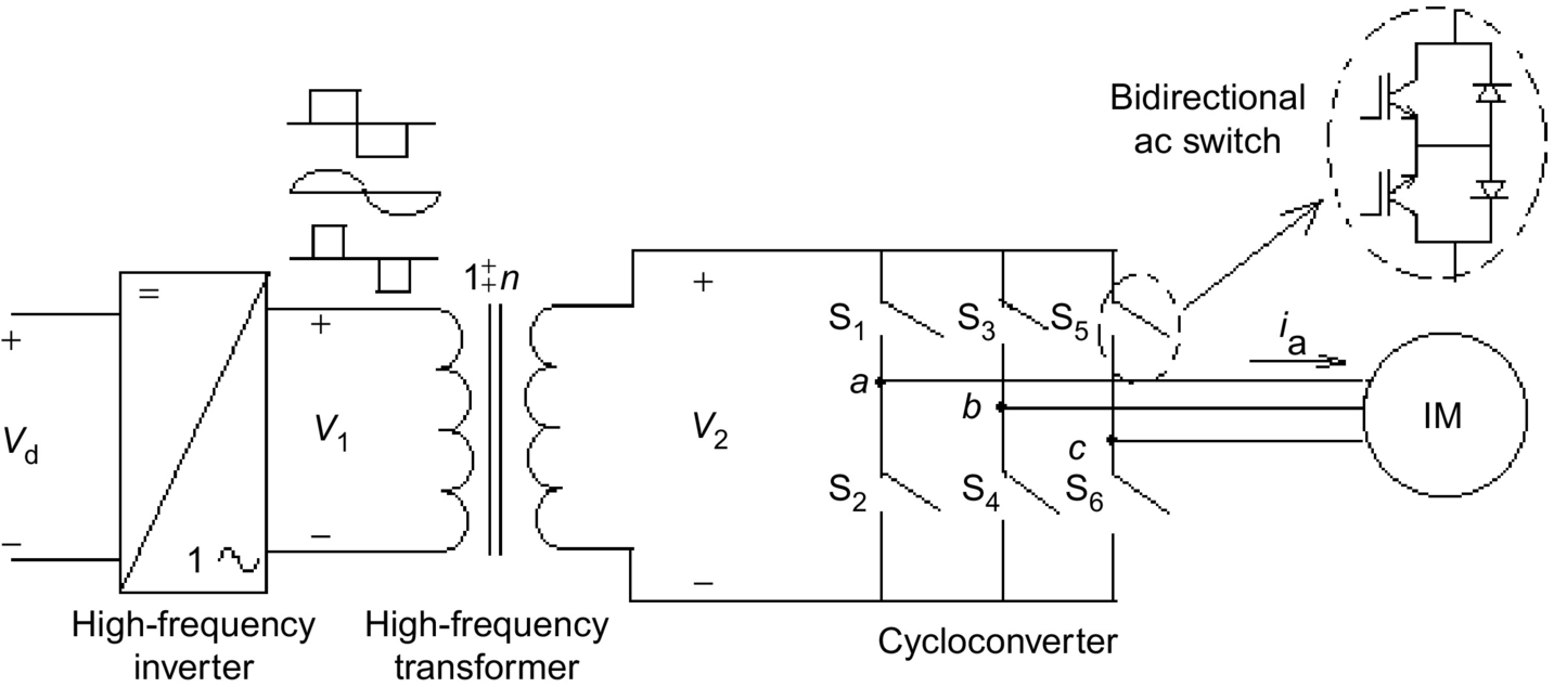
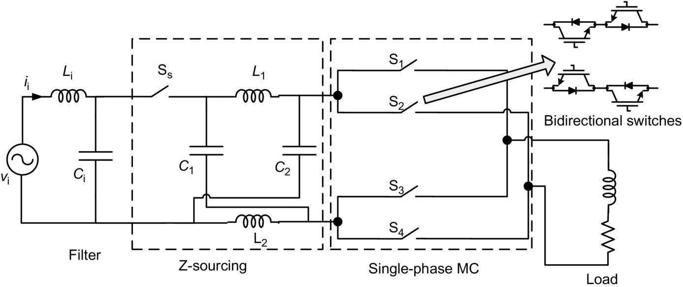
14.6.1 High Frequency Integral-Pulse Cycloconverter
The input to these converters may be sinusoidal or quasi square wave, and it is possible to use integral half-cycle pulse-width modulation (IPM) principle to synthesize the output voltage waves. The advantage is that the devices can be switched at zero voltage reducing the switching loss. This converter can only work at output frequency, which are multiples of the input frequency [90].
14.6.2 High-Frequency Phase-Controlled Cycloconverter
Here, phase control principle as explained earlier is used to synthesize the output voltage. A sawtooth carrier wave is compared with the sine modulating wave to generate the firing instants of the switches. The phase control provides switching at zero current reducing switching loss, but this scheme has more complex control circuit compared with the previous one. However, it can work at any frequency [91].