
Active Power Filters
Luis Morán University of Concepción, Concepción, Chile
Juan Dixon Catholic University of Chile, Santiago, Chile
Miguel Torres University of O'Higgins, Rancagua, Chile
Abstract
The growing number of power-electronics-based equipment has produced an important impact on the quality of electric power supply. Both high-power industrial loads and domestic loads cause harmonics in the network voltages. At the same time, much of the equipment causing the disturbances is quite sensitive to deviations from the ideal sinusoidal line voltage. Therefore, power quality problems may originate in the system or may be caused by the consumer itself. For an increasing number of applications, conventional equipment is proving insufficient for mitigation of power quality problems. Harmonic distortion has traditionally been dealt with the use of passive LC filters. However, the application of passive filters for harmonic reduction may result in parallel resonances with the network impedance, over compensation of reactive power at fundamental frequency, and poor flexibility for dynamic compensation of different frequency harmonic components. The increased severity of power quality in power networks has attracted the attention of power engineers to develop dynamic and adjustable solutions to the power quality problems. Such equipment, generally known as active filters, are also called active power line conditioners and are able to compensate current and voltage harmonics and reactive power, regulate terminal voltage, suppress flicker, and improve voltage balance in three-phase systems. The advantage of active filtering is that it automatically adapts to changes in the network and load fluctuations. They can compensate for several harmonic orders, and are not affected by major changes in network characteristics, eliminating the risk of resonance between the filter and network impedance. Another plus is that they take up very little space compared with traditional passive compensators.
Keywords:
Power electronics; Active filters; Power quality; Harmonics; Power compensation
Acknowledgments
The authors would like to acknowledge the financial support from “FONDECYT” through the 1140419 project. The collaboration of Dr. Pablo Acuña from the University of New South Wales, Sydney, Australia, is also recognized.
41.1 Introduction
The growing number of power-electronics-based equipment has produced an important impact on the quality of electric power supply. Both high-power industrial loads and domestic loads cause harmonics in the network voltages. At the same time, much of the equipment causing the disturbances is quite sensitive to deviations from the ideal sinusoidal line voltage. Therefore, power quality problems may originate in the system or may be caused by the consumer itself. Moreover, in the last years, the growing concern related to power quality comes from the following:
• Consumers that are becoming increasingly aware of the power quality issues and being more informed about the consequences of harmonics, interruptions, sags, switching transients, etc. Motivated by deregulation, they are challenging the energy suppliers to improve the quality of the power delivered.
• The proliferation of load equipment with microprocessor-based controllers and power electronic devices that are sensitive to many types of power quality disturbances.
• Emphasis on increasing overall process productivity that has led to the installation of high-efficiency equipment, such as adjustable speed drives and power factor correction equipment. This in turn has resulted in an increase in harmonics injected into the power system, causing concern about their impact on the system behavior.
For an increasing number of applications, conventional equipment is proving insufficient for the mitigation of power quality problems. Harmonic distortion has traditionally been dealt with the use of passive LC filters. However, the application of passive filters for harmonic reduction may result in parallel resonances with the network impedance, over compensation of reactive power at fundamental frequency, and poor flexibility for dynamic compensation of different frequency harmonic components.
The increased severity of power quality in power networks has attracted the attention of power engineers to develop dynamic and adjustable solutions to the power quality problems. Such equipment, generally known as active filters, are also called active power line conditioners and are able to compensate current and voltage harmonics and reactive power, regulate terminal voltage, suppress flicker, and improve voltage balance in three-phase systems. The advantage of active filtering is that it automatically adapts to changes in the network and load fluctuations. They can compensate for several harmonic orders, and are not affected by major changes in network characteristics, eliminating the risk of resonance between the filter and network impedance. Another plus is that they take up very little space compared with traditional passive compensators.
41.2 Types of Active Power Filters
The technology of active power filter has been developed during the past two decades reaching maturity for harmonic compensation, reactive power, and voltage balance in ac power networks. All active power filters are developed with pulse-width-modulated (PWM) converters (current-source or voltage-source inverters). The current-fed PWM inverter bridge structure behaves as a nonsinusoidal current source to meet the harmonic current requirement of the nonlinear load. It has a self-supported dc reactor that ensures the continuous circulation of the dc current. They present good reliability but have important losses and require higher values of parallel capacitor filters at the ac terminals to remove unwanted current harmonics. Moreover, they cannot be used in multilevel or multistep mode configurations to allow compensation in higher power ratings.
The other converter used in active power filter topologies is the PWM voltage-source inverter (PWM-VSI). This converter is more convenient for active power filtering applications since it is lighter, cheaper, and expandable to multilevel and multistep versions, to improve its performance for high power rating compensation with lower switching frequencies. The PWM-VSI has to be connected to the ac mains through coupling reactors. An electrolytic capacitor keeps a dc voltage constant and ripple-free.
Active power filters can be classified based on the type of converter, topology, control scheme, and compensation characteristics. The most popular classification is based on the topology such as shunt, series, or hybrid. The hybrid configuration is a combination of passive and active compensation. The different active power filter topologies are shown in Fig. 41.1.

Shunt active power filters (Fig. 41.1A) are widely used to compensate current harmonics, reactive power, and load current unbalanced. It can also be used as a static var generator in power system networks for stabilizing and improving voltage profile. Series active power filters (Fig. 41.1B) is connected before the load in series with the ac mains, through a coupling transformer to eliminate voltage harmonics and to balance and regulate the terminal voltage of the load or line. The hybrid configuration is a combination of series active filter and passive shunt filter (Fig. 41.1C). This topology is very convenient for the compensation of high-power systems, because the rated power of the active filter is significantly reduced (about 10% of the load size), since the major part of the hybrid filter consists of the passive shunt LC filter used to compensate lower-order current harmonics and reactive power at fundamental frequency.
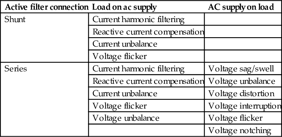
Due to the operation constraint, shunt or series active power filters can compensate only specific power quality problems. Therefore, the selection of the type of active power filter to improve power quality depends on the source of the problem as can be seen in Table 41.1.
Table 41.1
Active filter solutions to power quality problems
| Active filter connection | Load on ac supply | AC supply on load |
| Shunt | Current harmonic filtering | |
| Reactive current compensation | ||
| Current unbalance | ||
| Voltage flicker | ||
| Series | Current harmonic filtering | Voltage sag/swell |
| Reactive current compensation | Voltage unbalance | |
| Current unbalance | Voltage distortion | |
| Voltage flicker | Voltage interruption | |
| Voltage unbalance | Voltage flicker | |
| Voltage notching |
The principles of operation of shunt, series, and hybrid active power filters are described in the following sections.
41.2.1 Shunt Active Power Filters
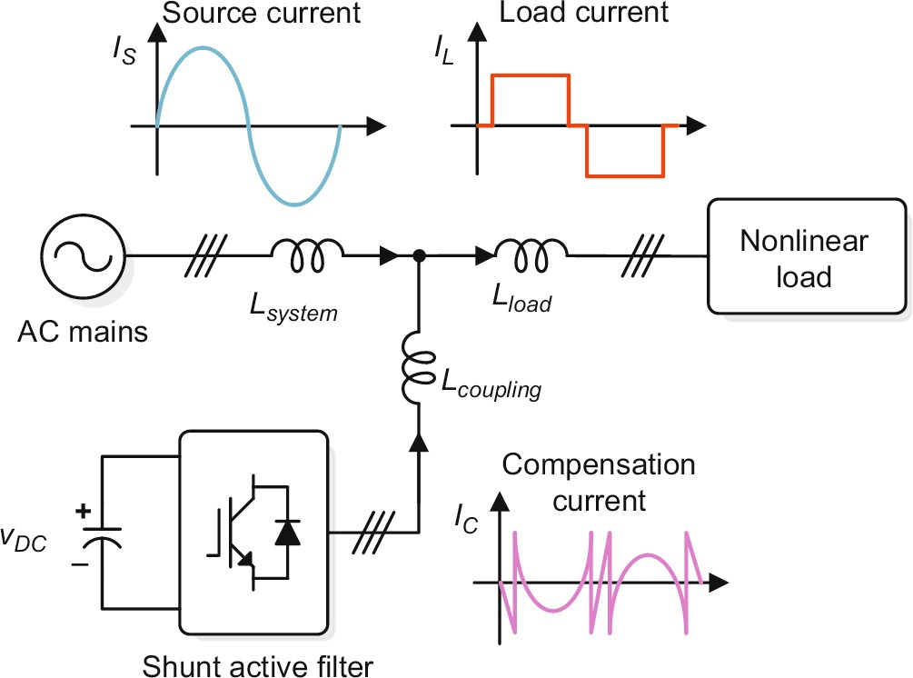
Shunt active power filters compensate current harmonics by injecting equal but opposite harmonic compensating current. In this case, the shunt active power filter operates as a current source injecting the harmonic components generated by the load but phase shifted by 180 degrees. As a result, components of harmonic currents contained in the load current are canceled by the effect of the active filter, and the source current remains sinusoidal and in phase with the respective phase-to-neutral voltage. This principle is applicable to any type of load considered as a harmonic source. Moreover, with an appropriate control scheme, the active power filter can also compensate the load power factor. In this way, the power distribution system sees the nonlinear load and the active power filter as an ideal resistor. The compensation characteristics of the shunt active power filter are shown in Fig. 41.2.
41.2.2 Power Circuit Topologies
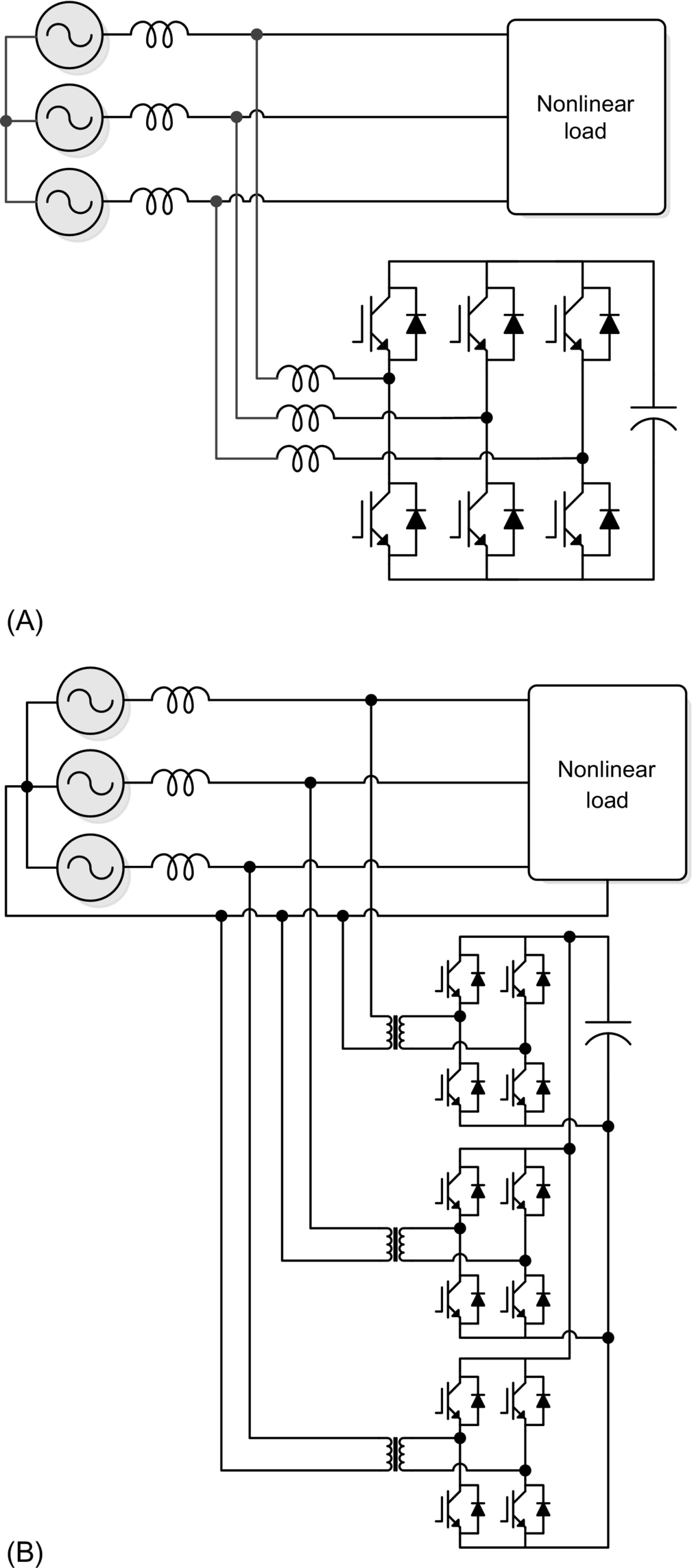
Shunt active power filters are normally implemented with PWM-VSIs. In this type of application, the PWM-VSI operates as a current-controlled voltage source. Traditionally, two-level PWM-VSIs have been used to implement such system connected to the ac bus through a transformer. This type of configuration is aimed to compensate nonlinear load rated in the medium power range (hundreds of kilovolt-amperes) due to semiconductor rated value limitations. However, in the last years, multilevel PWM-VSIs have been proposed to develop active power filters for medium-voltage and higher rated power applications. Also, active power filters implemented with multiple VSIs connected in parallel to a dc bus but in series through a transformer or in cascade have been proposed in the technical literature. The different power circuit topologies are shown in Fig. 41.3.
The use of VSI connected in cascade is an interesting alternative to compensate high-power nonlinear loads. The use of two PWM-VSI with different rated power allows the use of different switching frequencies, reducing switching stresses and commutation losses in the overall compensation system. The power circuit configuration of such a system is shown in Fig. 41.4.
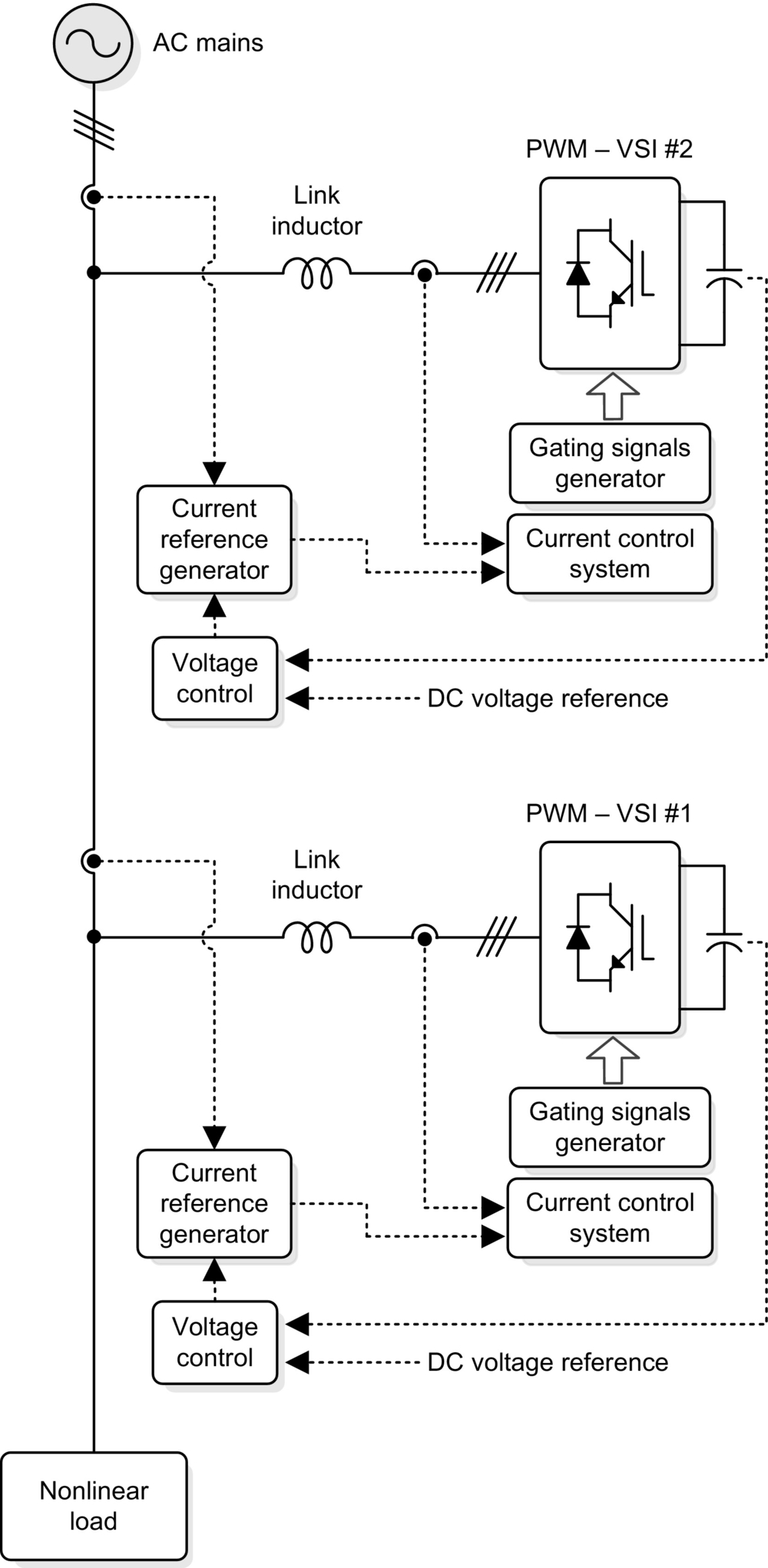
The VSI connected closer to the load compensates for the displacement power factor and lower-frequency current harmonic components (Fig. 41.5B), while the second compensates only high-frequency current harmonic components. The first converter requires higher rated power than the second and can operate at lower switching frequency. The compensation characteristics of the cascade shunt active power filter are shown in Fig. 41.5.

In recent years, there has been an increasing interest in using multilevel inverters for high-power energy conversion, especially for drives and reactive power compensation. The use of neutral-point-clamped (NPC) inverters (Fig. 41.6) allows equal voltage shearing of the series-connected semiconductors in each phase. Basically, multilevel inverters have been developed for applications in medium-voltage ac motor drives and static var compensation. For these types of applications, the output voltage of the multilevel inverter must be able to generate an almost sinusoidal output current. In order to generate a near sinusoidal output current, the output voltage should not contain low-frequency harmonic components.
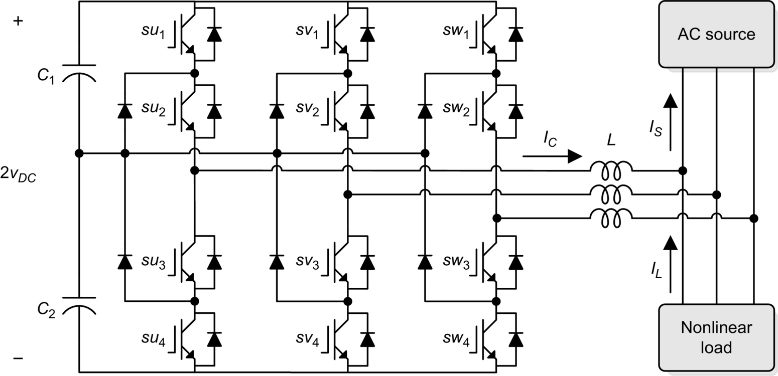
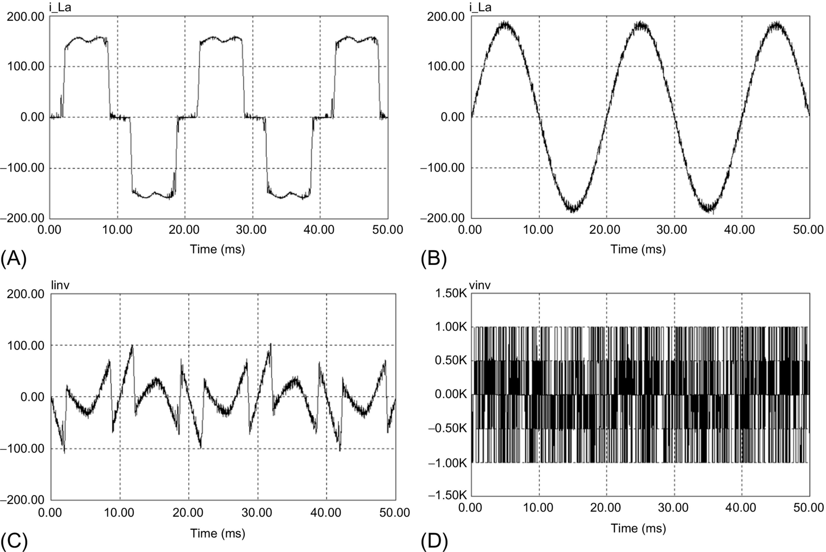
However, for active power filter applications, the three-level NPC inverter output voltage must be able to generate an output current that follows the respective reference current containing the harmonic and reactive component required by the load. Current and voltage waveforms obtained for a shunt active power filter implemented with a three-level NPC-VSI are shown in Fig. 41.7.
41.2.3 Control Scheme
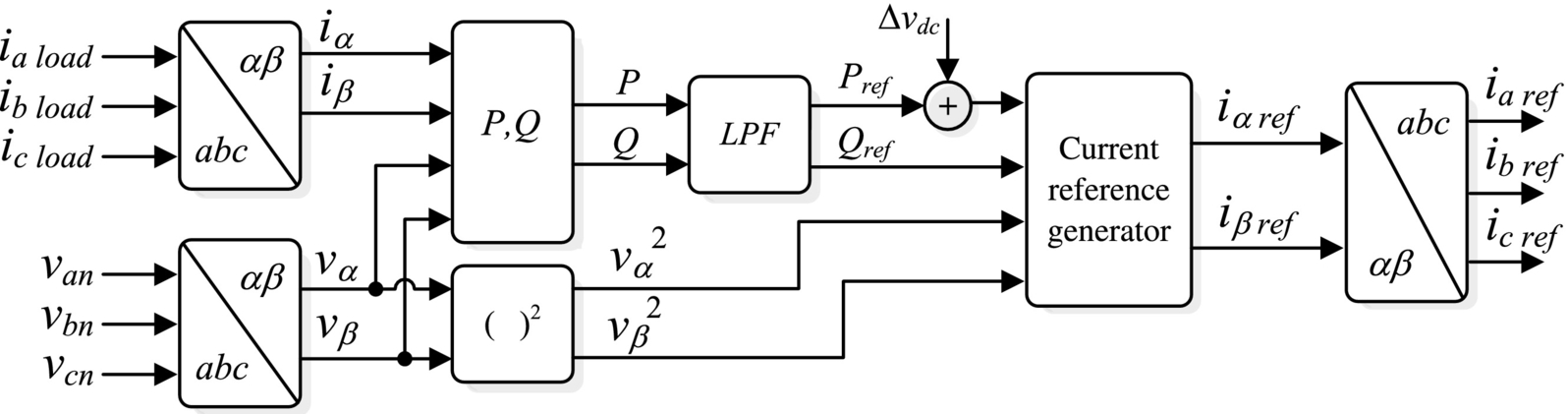
The control scheme of a shunt active power filter must calculate the current reference waveform for each phase of the inverter, maintain the dc voltage constant, and generate the inverter gating signals. The block diagram of the control scheme of a shunt active power filter is shown in Fig. 41.8.
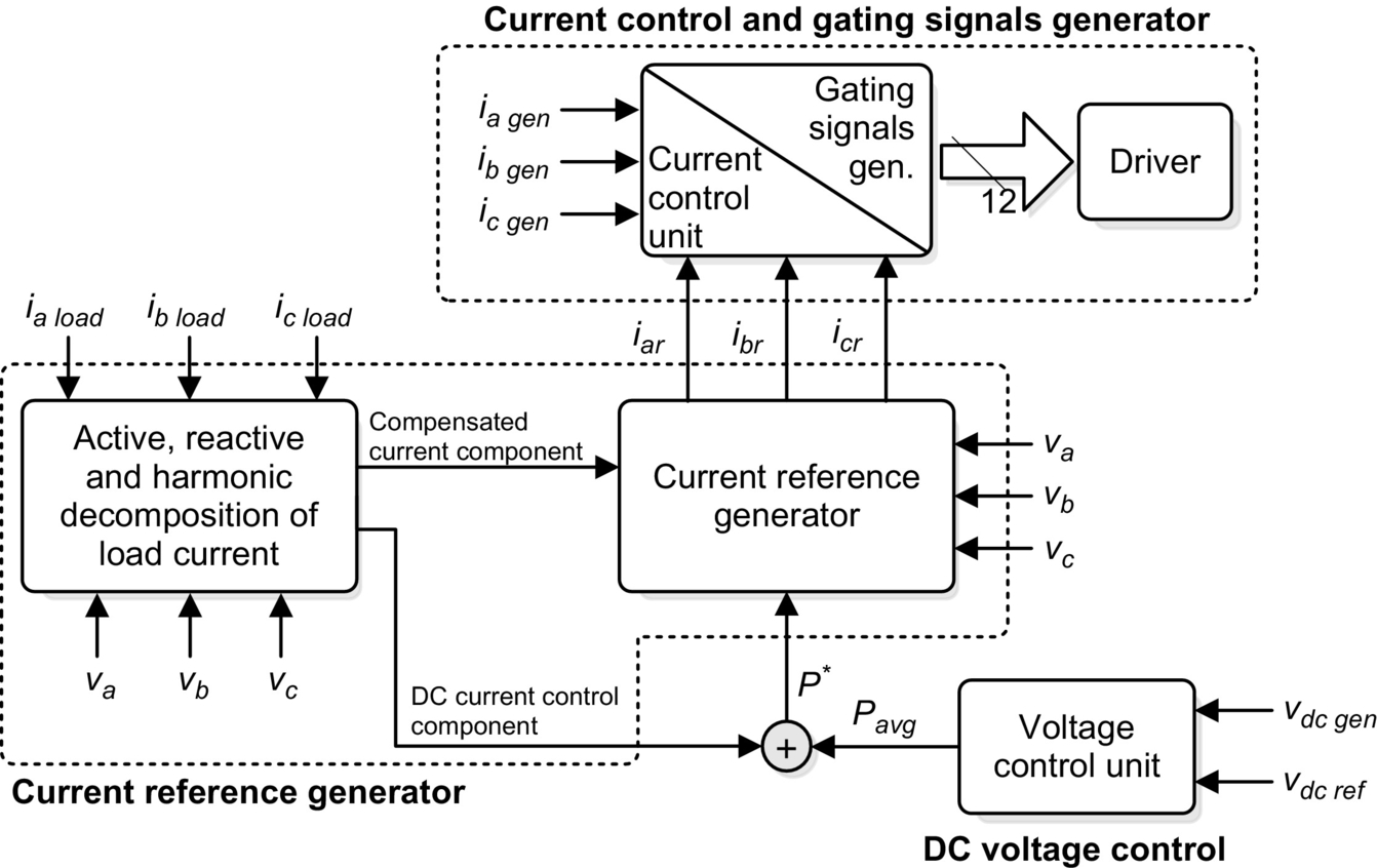
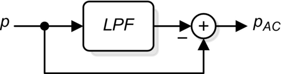
The current reference circuit generates the reference currents required to compensate the load current harmonics and reactive power and also try to maintain constant the dc voltage across the electrolytic capacitors. There are many possibilities to implement this type of control, and the most popular of them will be explained in this chapter. Also, the compensation effectiveness of an active power filter depends on its ability to follow with a minimum error and time delay the reference signal calculated to compensate the distorted load current. Finally, the dc voltage control unit must keep the total dc bus voltage constant and equal to a given reference value. The dc voltage control is achieved by adjusting the small amount of real power absorbed by the inverter. This small amount of real power is adjusted by changing the amplitude of the fundamental component of the reference current.
41.2.3.1 Current Reference Generation
There are many possibilities to determine the reference current required to compensate the nonlinear load. Normally, shunt active power filters are used to compensate the displacement power factor and low-frequency current harmonics generated by nonlinear loads. One alternative to determine the current reference required by the VSI is the use of the instantaneous reactive power theory, proposed by Akagi [1], the other one is to obtain current components in d-q or synchronous reference frame [2], and the third one is to force the system line current to follow a perfectly sinusoidal template in phase with the respective phase-to-neutral voltage.
Instantaneous reactive power theory
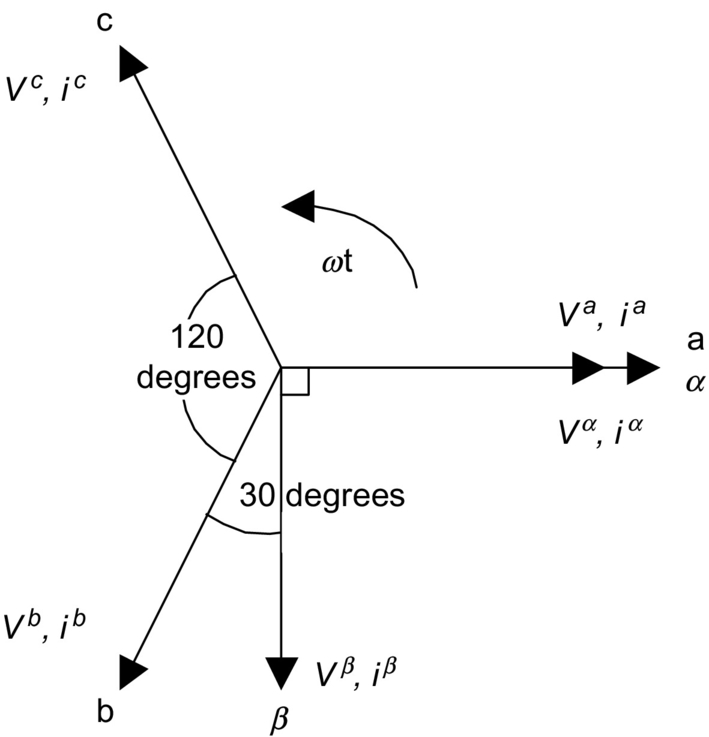
This concept is very popular and useful for this type of application and basically consists of a variable transformation from the a, b, c reference frame of the instantaneous power, voltage, and current signals to the α, β reference frame. The transformation equations from the a, b, c reference frame to the α, β coordinates can be derived from the phasor diagram shown in Fig. 41.9.
The instantaneous values of voltages and currents in the α, β coordinates can be obtained from the following equations:
[vαvβ]=[A]⋅[vavbvc][iαiβ]=[A]⋅[iaibic]

where A is the transformation matrix, derived from Fig. 41.9 and is equal to
[A]=√23[1−1/2−1/20√3/2−√3/2]

This transformation is valid if and only if va(t)+vb(t)+vc(t)![]() is equal to zero and also if the voltages are balanced and sinusoidal. The instantaneous active and reactive power in the α, β coordinates are calculated with the following expressions:
is equal to zero and also if the voltages are balanced and sinusoidal. The instantaneous active and reactive power in the α, β coordinates are calculated with the following expressions:
p(t)=vα(t)⋅iα(t)+vβ(t)⋅iβ(t)
q(t)=−vα(t)⋅iβ(t)+vβ(t)⋅iα(t)
It is evident that p(t) becomes equal to the conventional instantaneous real power defined in the a, b, c reference frame. However, in order to define the instantaneous reactive power, Akagi introduces a new instantaneous space vector defined by expression (41.4) or by the vector equation:
q=vαxiβ+vβxiα
where the vector q is perpendicular to the plane of α, β coordinates, to be faced in compliance with a right-hand rule; vα is perpendicular to iβ; and vβ is perpendicular to iα. The physical meaning of the vector q is not “instantaneous power” because of the product of the voltage in one phase and the current in the other phase. On the contrary, vαiα and vβiβ in Eq. (41.3) obviously mean “instantaneous power” because of the product of the voltage in one phase and the current in the same phase. Akagi named the new electric quantity defined in Eq. (41.5) “instantaneous imaginary power,” which is represented by the product of the instantaneous voltage and current in different axes, but cannot be treated as a conventional quantity.
The expression of the currents in the α−β![]() plane, as a function of the instantaneous power, is given by the following equation:
plane, as a function of the instantaneous power, is given by the following equation:
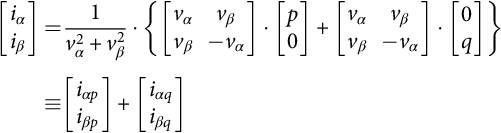
[iαiβ]=1v2α+v2β⋅{[vαvβvβ−vα]⋅[p0]+[vαvβvβ−vα]⋅[0q]}≡[iαpiβp]+[iαqiβq]
and the different components of the currents in the α−β![]() plane are shown in the following expressions:
plane are shown in the following expressions:
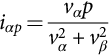
iαp=vαpv2α+v2β
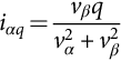
iαq=vβqv2α+v2β
iβp=vβpv2α+v2β

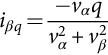
iβq=−vαqv2α+v2β
From Eqs. (41.3) and (41.4), the values of p and q can be expressed in terms of the dc components and the ac components, that is,
p=ˉp+˜p
q=ˉq+˜q
where
ˉp![]() is the dc component of the instantaneous power p and is related to the conventional fundamental active current,
is the dc component of the instantaneous power p and is related to the conventional fundamental active current,
˜p![]() is the ac component of the instantaneous power p; it does not have average value and is related to the harmonic currents caused by the ac component of the instantaneous real power.
is the ac component of the instantaneous power p; it does not have average value and is related to the harmonic currents caused by the ac component of the instantaneous real power.
ˉq![]() is the dc component of the imaginary instantaneous power q and is related to the reactive power generated by the fundamental components of voltages and currents.
is the dc component of the imaginary instantaneous power q and is related to the reactive power generated by the fundamental components of voltages and currents.
˜q![]() is the ac component of the instantaneous imaginary power q and it is related to the harmonic currents caused by the ac component of instantaneous reactive power.
is the ac component of the instantaneous imaginary power q and it is related to the harmonic currents caused by the ac component of instantaneous reactive power.
In order to compensate reactive power (displacement power factor) and current harmonics generated by nonlinear loads, the reference signal of the shunt active power filter must include the values of ˜p![]() , ˉq
, ˉq![]() , and ˜q
, and ˜q![]() . In this case, the reference currents required by the shunt active power filters are calculated with the following expression:
. In this case, the reference currents required by the shunt active power filters are calculated with the following expression:
[i⁎c,αi⁎c,β]=1v2α+v2β⋅[vαvβvβ−vα]⋅[˜pLˉqL+˜qL]
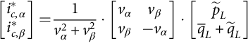
The final compensating currents including the zero-sequence components in a, b, c reference frame are the following:
[i⁎c,ai⁎c,bi⁎c,c]=√23⋅[1√2101√2−12√321√2−12−√32]⋅[−i0i⁎c,αi⁎c,β]

where the zero-sequence current component i0 is equal to 1√3(ia+ib+ic)![]() . The block diagram of the circuit required to generate the reference currents defined in Eq. (41.14) is shown in Fig. 41.10.
. The block diagram of the circuit required to generate the reference currents defined in Eq. (41.14) is shown in Fig. 41.10.
The advantage of instantaneous reactive power theory is that real and reactive power associated with fundamental components are dc quantities. These quantities can be extracted with a low-pass filter. Since the signal to be extracted is dc, filtering of the signal in the α−β![]() reference frame is insensitive to any phase-shift errors introduced by the low-pass filter, improving compensation characteristics of the active power filter. The same advantage can be obtained by using the synchronous reference frame method, proposed in [2]. In this case, transformation from a, b, c axes to d-q synchronous reference frame is done.
reference frame is insensitive to any phase-shift errors introduced by the low-pass filter, improving compensation characteristics of the active power filter. The same advantage can be obtained by using the synchronous reference frame method, proposed in [2]. In this case, transformation from a, b, c axes to d-q synchronous reference frame is done.
Effects of the low-pass filter design characteristics in compensation performance
A Butterworth filter is normally used due to the adequate frequency response. A second-order filter offers an appropriate relation between the transient response and the required attenuation characteristic. Higher-order filters achieve better filtering characteristic, but the settling time is increased. Since the low-pass filter cannot eliminate completely the low-frequency harmonic contained in the p and q signals, the shunt active power filter cannot compensate the entire low-frequency harmonic contained in the load current. Normally, the cutoff frequency is equal to 127 Hz with an attenuation factor of 15 dB for the first ac component to be eliminated, which means an 82.2% attenuation of the fifth and seventh harmonic components (Fig. 41.11). The expression that relates the system line current harmonic distortion with the LPF cutoff frequency and load power factor is shown in Eq. (41.15):
THDisys=√∞∑h=6k1(fn/fc)4+1[((h2+1)/(h2−1))−(1/(h2−1))cos(2φ)]cos(φ)
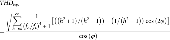
with k=1, 2, 3,… and fh is the frequency of the harmonic component of order h and fc is the LPF cutoff frequency.
Fig. 41.12 shows the total harmonic distortion (THD) in the line currents introduced by the second-order Butterworth filtering characteristics, as a function of the cutoff frequency and considering a 50 Hz ac mains frequency. The harmonic distortion of the compensated line current depends on the load displacement power factor, as shown in Eq. (41.15). If the cutoff frequency of the low-pass filter is changed, the active power filter compensation performance is affected and the transient response of the control scheme.

 .
.Effects of the supply voltage distortion in compensation performance
One of the most important characteristics of the instantaneous imaginary power concept is that in order to obtain the current reference signal required to compensate reactive and harmonic current components, the system phase-to-neutral voltages are used. In general, purely sinusoidal voltages are considered in previously reported analysis. In case voltage is purely sinusoidal, the dc components of p and q in the α–β plane are related with the fundamental components in the real a, b, c reference system. This is not the case if the system voltages are distorted or unbalanced, as it is demonstrated below.
It is assumed that the supply voltages have harmonic distortion, and these are represented by
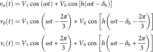
va(t)=V1cos(ωt)+Vhcos[h(ωt−δh)]vb(t)=V1cos(ωt−2π3)+Vhcos[h(ωt−δh−2π3)]vc(t)=V1cos(ωt+2π3)+Vhcos[h(ωt−δh+2π3)]
Since the harmonic voltage component introduces a dc component in p and q, compensation performance of the shunt active power filter is reduced, as shown in Fig. 41.13. The larger the harmonic distortion in the system voltage is, the active power filter performance is more affected.
 .
.Effects of the supply voltage unbalance in compensation performance
Voltage unbalance also affects the active power filter compensation performance. In this analysis, the phase-to-neutral voltages of the ac supply are equal to
va(t)=V1cos(ωt)vb(t)=V1(1+m)cos(ωt−2π3)vc(t)=V1(1−m)cos(ωt+2π3)

with 0<m<1![]() .
.
If the low-pass filter is considered as ideal and the active filter follows exactly the current references, the compensated supply current (phase a) is
iSa=I1cos(φ)cos(ωt)+√33m[I1sin(φ)cos(3ωt)+I1,,cos,,(3ωt−φ)]
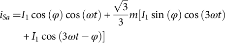
In this case, the active power filter is not able to fully compensate the system line current, since compensation performance depends on the voltage unbalance magnitude.
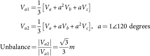
The unbalance is defined as a function of the positive and negative-sequence component as
Va1=13[Va+a2Vb+aVc]Va2=13[Va+aVb+a2Vc],a=1∠120degreesUnbalance=|Va2||Va1|=√33m
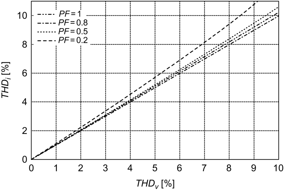
The harmonic distortion is equal to
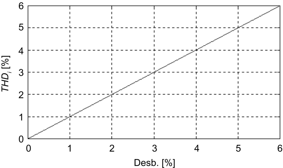
THDi=√33m
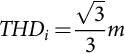
The relation between line current harmonic distortion and voltage unbalance is shown in Fig. 41.14.
Effects of the time delay introduced by the dsp in compensation performance
If a DSP is used to derive the reference generation signals, a time delay, T, associated with the processing time is introduced in the calculation of the reference signals. Considering a simultaneous sampling, the ac mains compensated line current with an ideal low-pass filter in the control scheme (phase a) is
iSa=I1cos(ωt)[cos(φ)+sin(ωT)]+ΔVDCcos(ωt)+∞∑n=2k−1In[1−cos(nωT)]cos[n(ωt−φ)]+∞∑n=2k−1Insin(nωT)sin[n(ωt−φ)]
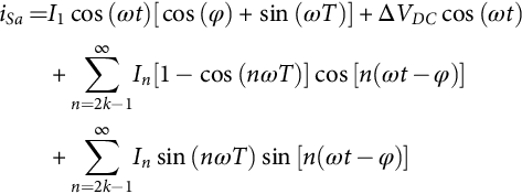
The time delay introduced by the DSP affects the compensation performance, especially when fast changes are present in the load current. Nevertheless, when T is small (T>50s![]() ), the effect in compensation performance is negligible.
), the effect in compensation performance is negligible.
In four-wire systems, unbalances in the load current also affect the generation of the adequate current reference signal that will assure high-performance active power filter compensation. This assumption can be proved by considering the following load currents:
iLa=I1cos(ωt−φ)+∞∑n=2k−1Incos[n(ωt−φ)]iLb=I1(1+l)cos(ωt−φ−2π3)+∞∑n=2k−1In(1+l)cos[n(ωt−φ−2π3)]iLc=I1(1−l)cos(ωt−φ+2π3)+∞∑n=2k−1In(1−l)cos[n(ωt−φ+2π3)]iLN=iLa+iLb+iLc
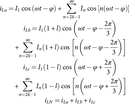
with 0<l<1![]() , k=1, 2, 3,…
, k=1, 2, 3,…
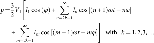
Eq. (41.23) shows the presence of low-frequency even harmonics in the active power expression introduced by the load current unbalanced. These low-frequency current components force to reduce the cutoff frequency of the low-pass filter, close to 100 Hz, which affects the transient response of the active power filter:
p=32V1[I1cos(φ)+∞∑n=2k−1Incos[(n+1)ωt−nφ]+∞∑m=2k−1,Im,,cos,,[(m−1)ωt−mφ]]withk=1,2,3,…
Synchronous reference frame algorithm
The block diagram of a current reference generator that uses the synchronous reference frame algorithm is shown in Fig. 41.15.
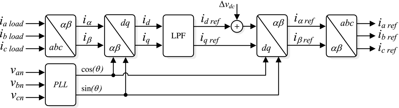
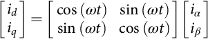
In this case, the real currents are transformed into a synchronous reference frame [2]. The reference frame is synchronized with the ac mains voltage and is rotating at the same frequency. The transformation is defined by
[idiq]=[cos(ωt)sin(ωt)sin(ωt)cos(ωt)][iαiβ]
As for the instantaneous reactive power theory, d and q terms are composed by a dc and multiple ac components, such as id=iddc+idac![]() and iq=iqdc+iqac
and iq=iqdc+iqac![]() . The compensation reference signals are obtained from the following expressions: idref=−idac
. The compensation reference signals are obtained from the following expressions: idref=−idac![]() and iqref=−iqdc−iqac
and iqref=−iqdc−iqac![]() . The compensated currents generated by the shunt active power filter are obtained from Eq. (41.25):
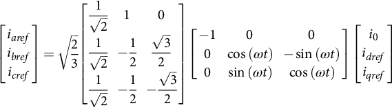
. The compensated currents generated by the shunt active power filter are obtained from Eq. (41.25):
[iarefibreficref]=√23[1√2101√2−12√321√2−12−√32][−1000cos(ωt)−sin(ωt)0sin(ωt)cos(ωt)][i0idrefiqref]
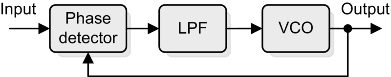
One of the most important characteristics of this algorithm is that the reference currents are obtained directly from the load currents without considering the source voltages. This is an important advantage since the generation of the reference signals is not affected by voltage unbalance or voltage distortion, therefore increasing the compensation robustness and performance. However, in order to transform from the α−β![]() plane to the d-q synchronous reference frame, sine and cosine signals synchronized with the respective phase-to-neutral voltages are required. A phase-locked loop (PLL) per each phase, as the one shown in Fig. 41.16, must be used.
plane to the d-q synchronous reference frame, sine and cosine signals synchronized with the respective phase-to-neutral voltages are required. A phase-locked loop (PLL) per each phase, as the one shown in Fig. 41.16, must be used.
Since the algorithm used to obtain the reference current presents the same mathematical procedure and operations that the ones required in the instantaneous reactive power concept, the effects introduced by the filter and DSP time delay are similar. Unbalanced load currents generate a different harmonic spectrum in the synchronous reference frame, and low-order harmonic components appear in the reference signal. In order to separate these uncharacteristic low-frequency current components, the cutoff frequency of the low-pass filter must be reduced.
Peak detection method
There are other possibilities to generate the current reference signal required to compensate reactive power and current harmonics. Basically, all the different schemes try to obtain the current reference signals that include the reactive components required to compensate the displacement power factor and the current harmonics generated by the nonlinear load. Fig. 41.17 shows another scheme used to generate the current reference signals required by a shunt active power filter. In this case, the ac current generated by the inverter is forced to follow the reference signal obtained from the current reference generator. In this circuit, the distorted load current is filtered, extracting the fundamental component, il1. The band-pass filter is tuned at the fundamental frequency (50 or 60 Hz), so that the gain attenuation introduced in the filter output signal is zero and the phase-shift angle is 180 degrees. Thus, the filter output current is exactly equal to the fundamental component of the load current but phase shifted by 180 degrees. If the load current is added to the fundamental current component obtained from the second-order band-pass filter, the reference current waveform required to compensate only harmonic distortion is obtained. In order to provide the reactive power required by the load, the current signal obtained from the second-order band-pass filter Il1 is synchronized with the respective phase-to-neutral source voltage (see Fig. 41.17) so that the inverter ac output current is forced to lead the respective inverter output voltage, thereby generating the required reactive power and absorbing the real power necessary to supply the switching losses and also to maintain the dc voltage constant.
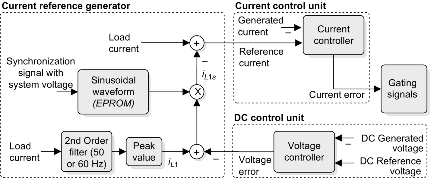
The real power absorbed by the inverter is controlled by adjusting the amplitude of the fundamental current reference waveform, Il1, obtained from the reference current generator. The amplitude of this sinusoidal waveform is equal to the amplitude of the fundamental component of the load current plus or minus the error signal obtained from the dc voltage control unit. In this way, the current signal allows the inverter to supply the current harmonic components, the reactive power required by the load, and to absorb the small amount of active power necessary to cover the switching losses and to keep the dc voltage constant (Fig. 41.18).
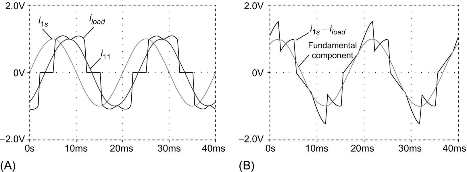
 , and its fundamental component.
The main characteristic of this method is the direct derivation of the compensating component from the load current, without the use of any reference frame transformation [1,2]. Nevertheless, this technique presents a low-frequency oscillation problem in the active power filter dc bus voltage. To improve this technique, a modification of the previous scheme (Fig. 41.17) is shown in Fig. 41.19. The scheme is necessary for each phase. The expression for iMa is
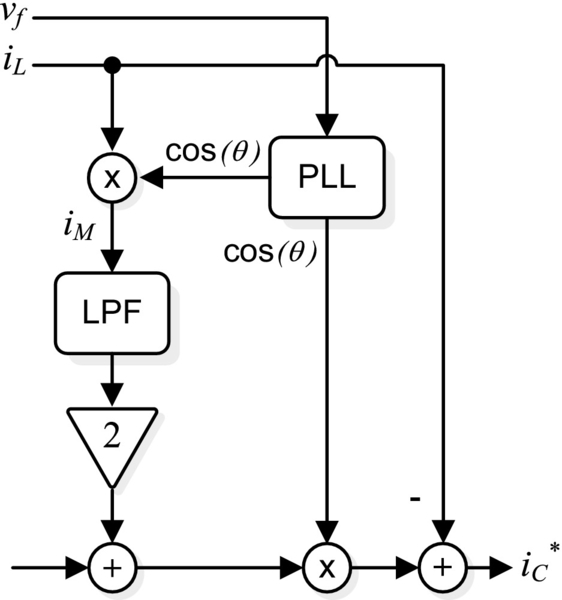
iMa=I1cos(φ)2+I1cos(2ωt−φ)2+∞∑n=2k−1In2{cos[(n−1)ωt−nφ]+cos,,[(n+1)ωt−nφ]}
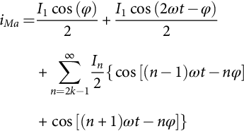
with k=1, 2, 3,…
Fig. 41.20 shows the current harmonic distortion introduced by the low-pass filter used in the control scheme and the associated cutoff frequency. The current distortion of the compensated current depends on the phase angle of the fundamental load current component.

The supply voltage has no effect on the reference current generation. Synchronization with the ac mains voltage is the important issue in this scheme and in the synchronous reference frame theory. Unbalanced loads do not affect the reference generation. Nevertheless, the method cannot achieve active power balance in four-wire systems. The control circuit implementation of the peak detection method is simple and does not require complex calculation, so the processing time on a DSP is lower than the required in the two previous implementations, (T<10 s). The use of this method minimizes the distortion introduced on current harmonics.
Technical comparison of the three different techniques
In order to validate the effectiveness of the proposed analysis, a common industrial system is considered. The results are obtained using the previous equations and Matlab simulation results. The DSP delay introduced is using the processing time according to the DSP ADSP2187. The parameters considered are
THDiL=29%THDV=5%cos(φ)=0.87Unbalance=3%
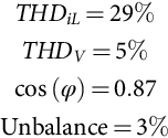
Table 41.2 shows the numeric results.
Table 41.2
Results of the considered case
| Technique | THDiS(%) | FP | Transient delay td (ms) |
| PQ | 8.2 | 0.99 | 18.1 |
| DQ | 3.1 | 0.99 | 18.1 |
| DPVM | 2.3 | 0.99 | 56.8 |
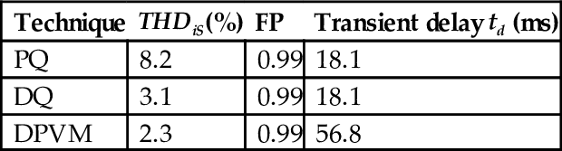
Table 41.3 shows a comparison of the three different techniques analyzed. The effects of the nonideal conditions are described for each technique.
Table 41.3
Comparison of the techniques
| Parameter | PQ | SRF | PDM |
| Load PF required to achieve full compensation | PF>0.3 |
PF>0.3 |
PF>0.2 |
| Harmonic distortion voltage effect on the compensated current | THDi≈THDv |
0 | 0 |
| Unbalanced voltage effect | THDi≈Unbalance |
0 | 0 |
| Dynamic response under load changes (in function of fc, td=5τ |
Fast (load balanced) | Fast (load balanced) | Slow |
| Capability of load balance | Yes (It is necessary to reduce cutoff frequency fc) | Yes (it is necessary to reduce cutoff frequency fc) | No |
| DSP delay time introduced | Minimum | Minimum | ≈0 |
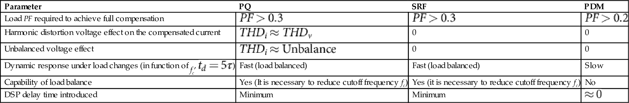
In conclusion, it can be mentioned that the compensation performance of the different techniques is similar under ideal conditions, but under the presence of unbalanced and voltage distortion, the synchronous reference frame algorithm presents the best performance, since it is insensitive to voltage perturbations. It is fundamental to consider adequately the cutoff frequency in the filter used to extract the ac component in the different techniques. If the frequency is changed, the compensation performance is affected as well as the transient response of the control scheme. In four-wire systems, unbalance in the load current also affects the generations of the adequate current reference. Unbalanced load currents generate a different harmonic spectrum in the dc reference frame, and low-order harmonic components appear in the reference signal; then, the cutoff frequency of the filter must be reduced.
41.2.3.2 Current Modulator
The effectiveness of an active power filter depends basically on the design characteristics of the current controller, the method implemented to generate the reference template and the modulation technique used. Most of the modulation techniques used in active power filters are based on PWM strategies. In this chapter, four of these methods, whose characteristics are their simplicity and effectiveness, are analyzed: periodical sampling control, hysteresis band control, triangular carrier control, and vector control. The first three methods have been tested with different waveform templates sinusoidal, quasisquare, and rectifier compensation current and were compared in terms of the harmonic content and distortion at the same switching frequency [3]. The analysis shows that for sinusoidal current generation the best method is triangular carrier, followed by hysteresis band and periodical sampling. For other types of references, however, one strategy may be better than the others. Also, it was shown that each control method is affected in a different way by the switching time delays present in the driving circuitry and in the power semiconductors.
Periodical sampling
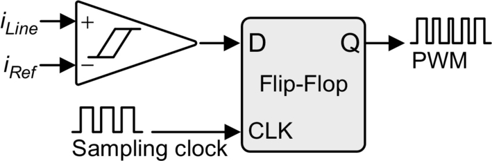
The periodical sampling method switches the power transistors of the converter during the transitions of a square-wave clock of fixed frequency (the sampling frequency). As shown in Fig. 41.21, this type of control is very simple to implement since it requires a comparator and a D-type flip-flop per phase. The main advantage of this method is that the minimum time between switching transitions is limited to the period of the sampling clock. However, the actual switching frequency is not clearly defined.
Hysteresis band
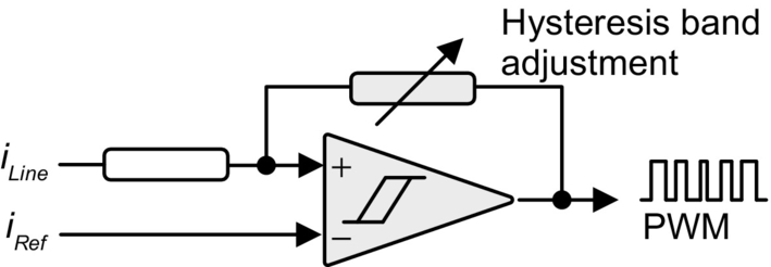
The hysteresis band method switches the transistors when the current error exceeds a fixed magnitude: the hysteresis band. As can be seen in Fig. 41.22, this type of control needs a single comparator with hysteresis per phase. In this case, the switching frequency is not determined, but it can be estimated.
Triangular carrier
The triangular carrier method, shown in Fig. 41.23, compares the current error with fixed-amplitude and fixed-frequency triangular wave (the triangular carrier). The error is processed through a proportional-integral (PI) gain stage before the comparison with the triangular carrier takes place. As can be seen, this control scheme is more complex than the periodical sampling and hysteresis band. The values for the PI control gain kp and ki determine the transient response and steady-state error of the triangular carrier method. It was found empirically that the values for kp and ki shown in Eqs. (41.27) and (41.28) give a good dynamic performance under transient- and steady-state operating conditions:
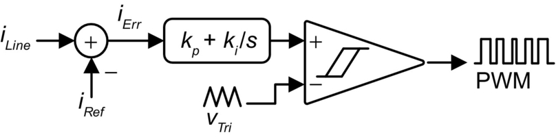
k⁎p=(L+Lo)⋅ωc2Vdc
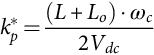
k⁎i=ωck⁎p
where L+Lo![]() is the total series inductance seen by the converter; ωc is the triangular carrier frequency, whose amplitude is 1 V peak-peak; and Vdc is the dc supply voltage of the inverter.
is the total series inductance seen by the converter; ωc is the triangular carrier frequency, whose amplitude is 1 V peak-peak; and Vdc is the dc supply voltage of the inverter.
Vector control technique
This current control technique proposed in [4] divides the α−β![]() reference frame of currents and voltages in six regions, phase shifted by 30 degrees (Fig. 41.24); identifies the region where the current vector error Δi is located; and selects the inverter output voltage vector Vinv that will force Δi to change in the opposite direction, keeping the inverter output current close to the reference signal.
reference frame of currents and voltages in six regions, phase shifted by 30 degrees (Fig. 41.24); identifies the region where the current vector error Δi is located; and selects the inverter output voltage vector Vinv that will force Δi to change in the opposite direction, keeping the inverter output current close to the reference signal.
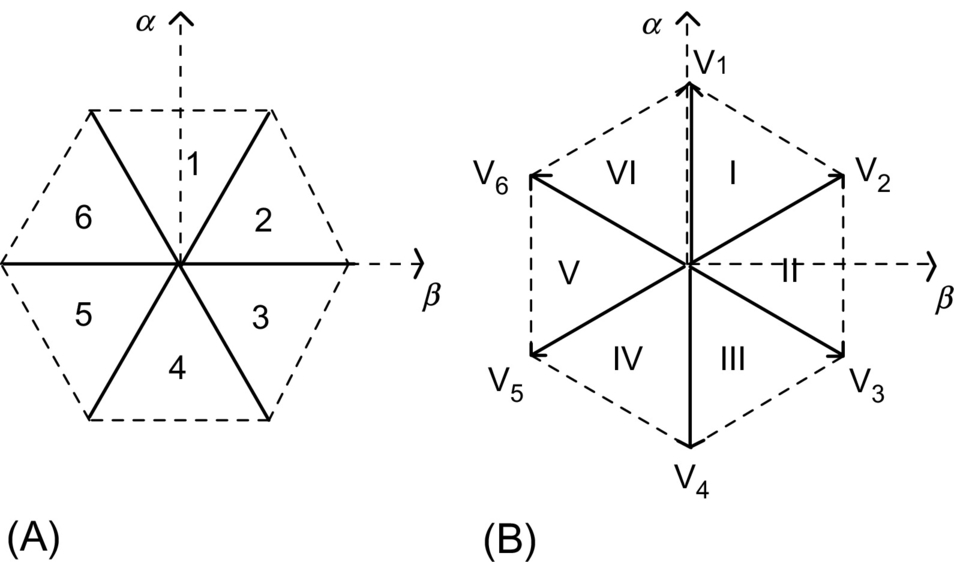
 reference frame by the current control scheme: (A) the hexagon defined by the inverter output current vector and (B) the hexagon defined by the inverter output voltage vector.
Fig. 41.25 shows the single-phase equivalent circuit of the shunt active power filter connected to a nonlinear load and to the power supply.
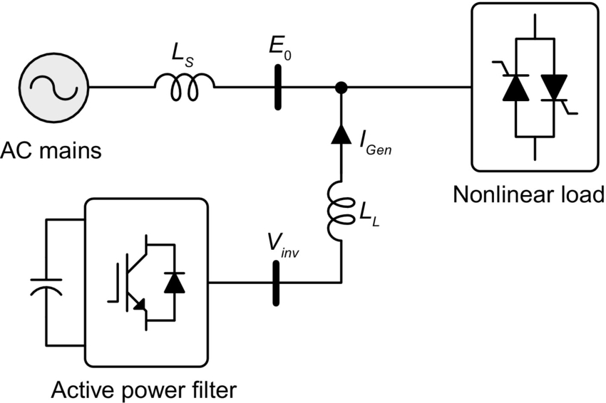
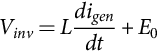
The equation that relates the active power filter currents and voltages is obtained by applying Kirchhoff law to the equivalent circuit shown in Fig. 41.25:
Vinv=Ldigendt+E0
The current error vector Δi is defined by the following expression:
Δi=iref−igen
where iref represents the inverter reference current vector defined by the instantaneous reactive power concept. By replacing Eq. (41.30) in Eq. (41.29),
Vinv=Lddt(iref−Δi)+E0⇒LdΔidt=Ldirefdt+E0−Vinv

If E=L(diref/dt)+E0![]() , then Eq. (41.31) becomes
, then Eq. (41.31) becomes
LdΔidt=E−Vinv
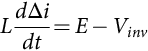
Eq. (41.32) represents the active power filter state equation and shows that the current error vector variation dΔi/dt is defined by the difference between the fictitious voltage vector E and the inverter output voltage vector Vinv. In order to keep dΔi/dt close to zero, Vinv must be selected near E0.
The selection of the inverters' gating signals is defined by the region in which Δi is located and by its amplitude. In order to improve the current control accuracy and associate time response, depending on the amplitude of Δi, the following actions are defined:
− If Δi≤δ![]() , the gating signals of the inverter are not changed.
, the gating signals of the inverter are not changed.
− If h≤Δi≤δ![]() , the inverter gating signals are defined following mode a.
, the inverter gating signals are defined following mode a.
− If Δi>h![]() , the inverter gating signals are defined following mode b.
, the inverter gating signals are defined following mode b.
where δ and h are reference values that define the accuracy and the hysteresis window of the current control scheme.
Mode a: Small changes in Δi(h≤Δi≤δ)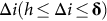
The selection of the inverter switching mode a can be explained with the following example. Assuming that the voltage vector E is located in region I (Fig. 41.26A) and the current error vector Δi is in region 6 (Fig. 41.26B), the inverter voltage vectors, Vinv, located closest to E are V1 and V2. The vectors E−V2![]() and E−V1
and E−V1![]() define two vectors LdΔi/dt, located in regions III and V, respectively, as shown in Fig. 41.26A, so in order to reduce the current vector error Δi, LdΔi/dt must be located in region III. Thus, the inverter output voltage has to be equal to V1. In this way, Δi will be forced to change in the opposite direction reducing its amplitude faster. By doing the same analysis for all the possible combinations, the inverter switching modes for each location of Δi and E can be defined (Table 41.4).
define two vectors LdΔi/dt, located in regions III and V, respectively, as shown in Fig. 41.26A, so in order to reduce the current vector error Δi, LdΔi/dt must be located in region III. Thus, the inverter output voltage has to be equal to V1. In this way, Δi will be forced to change in the opposite direction reducing its amplitude faster. By doing the same analysis for all the possible combinations, the inverter switching modes for each location of Δi and E can be defined (Table 41.4).

Table 41.4
Inverter switching modes
| E region | △i Region | |||||
| 1 | 2 | 3 | 4 | 5 | 6 | |
| I | V1 | V2 | V2 | V0−V7 |
V0−V7 |
V1 |
| II | V2 | V2 | V3 | V3 | V0−V7 |
V0−V7 |
| III | V0−V7 |
V3 | V3 | V4 | V4 | V0−V7 |
| IV | V0−V7 |
V0−V7 |
V4 | V4 | V5 | V5 |
| V | V6 | V0−V7 |
V0−V7 |
V5 | V5 | V6 |
| VI | V1 | V1 | V0−V7 |
V0−V7 |
V6 | V6 |
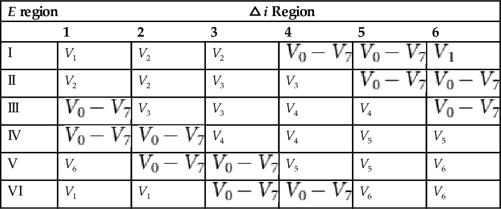
Vk represents the inverter switching functions defined in Table 41.5.
Mode b: Large changes in Δi(Δi>h)
If Δi becomes larger than h in a transient state, it is necessary to choose the switching mode in which the dΔi/dt has the largest opposite direction to Δi. In this case, the best inverter output voltage Vinv corresponds to the value located in the same region of Δi.
The switching frequency may be fixed by controlling the time between commutations and not applying a new switching pattern if the time between two successive commutations is lower than a selected value (t=1/2fc![]() ).
).
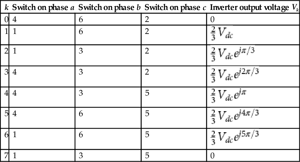
Fig. 41.27 shows the block diagram of the inverter vector current control scheme implemented in a microcontroller. In Fig. 41.27, ⁎E represents the region where the vector E is located, ⁎Δi, the region of Δi, k1 keeps the same value of k (no commutation in the inverter), k2 selects the new inverter output voltage from Table 41.4, and k3 selects Vinv in the same region of Δi.
41.2.3.3 Control Loop Design
Active power filters based on self-controlled dc bus voltage require two control loops, one to control the inverter output current and the other to regulate the inverter dc voltage. Different design criteria have been presented in the technical literature; however, a classic design procedure using a PI controller will be presented in this chapter. In general, the design procedure for the current and voltage loops is based on the respective time-response requirements. Since the transient response of the active power is determined by the current control loop, its time response has to be fast enough to follow the current reference waveform closely. On the other hand, the time response of the dc voltage does not need to be fast and is selected to be at least 10 times slower than the current control loop time response. Thus, these two control systems can be decoupled and designed as two independent systems.
A PI controller is normally used for the current and the voltage control loops since it contributes to zero steady-state error in tracking the reference current and voltage signals, respectively.
Design of the current control loop
The design of the current control loop gains depends on the selected current modulator. In the case of selecting the triangular carrier technique, to generate the gating signals, the error between the generated current and the reference current is processed through a PI controller, and then, the output current error is compared with a fixed-amplitude and fixed-frequency triangular wave (Fig. 41.23). The advantage of this current modulator technique is that the output current of the converter has well-defined spectral line frequencies for the switching frequency components.
Since the active power filter is implemented with a voltage-source inverter, the ac output current is defined by the inverter ac output voltage. The block diagram of the current control loop for each phase is shown in Fig. 41.28 where
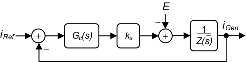
| E | phase-to-neutral source voltage, |
| Z(s) | impedance of the link reactor, |
| Ks | gain of the converter, and |
| Gc(s) | gain of the controller. |
The values of Ks and Gc(s) are given in Eqs. (41.33) and (41.34):
Ks=Vdc2ξ

Gc(s)=Kp+Kis
From Fig. 41.27 and Eq. (41.34), the following expression is obtained:
Igen=[Ks(Kp+(Ki/s))]/(Rr+sLr)1+[Ks(Kp+(Ki/s))/(Rr+sLr)]Iref−1/(Rr+sLr)1+(Ks(Kp+Ki/s)/(Rr+sLr))E
The characteristic equation of the current loop is given by
1+(Kps+Ki/s)s(Rr+sLr)
The analysis of the characteristic equation proves that the current control loop is stable for all values of Kp and Ki. Also, this analysis shows that Kp determines the speed response and Ki defines the damping factor of the control loop. If Kp is too big, the error signal can exceed the amplitude of the triangular waveform, affecting the inverter switching frequency, and if Ki is too small, the gain of the PI controller decreases, which means that the generated current will not be able to follow the reference current closely. The active filter transient response can be improved by adjusting the gain of the proportional part (Kp) to equal one and the gain of the integrator (Ki) to equal the frequency of the triangular waveform.
DC voltage control loop
Voltage control of the dc bus is performed by adjusting the small amount of real power flowing into the dc capacitor, thus compensating for the conduction and switching losses. The voltage loop is designed to be at least 10 times slower than the current loop, hence the two loops can be considered decoupled. The dc voltage control loop needs not to be fast, since it only responds for steady-state operating conditions. Transient changes in the dc voltage are not permitted and are taken into consideration with the selection criteria of the appropriate electrolytic capacitor value.
41.2.4 Power Circuit Design
The selection of the ac link reactor and the dc capacitor values affects directly the performance of the active power filter. Static var compensators implemented with voltage-source inverters present the same power circuit topology, but for this type of application, the criteria used to select the values of Lr and C are different. For reactive power compensation, the design of the synchronous link inductor, Lr, and the dc capacitor, C, is performed based on harmonic distortion constrain. That is, Lr must reduce the amplitude of the current harmonics generated by the inverter, while C must keep the dc voltage ripple factor below a given value. This design criteria cannot be applied in the active power filter since it must be able to generate distorted current waveforms. However, Lr must be specified so that it keeps the high-frequency switching ripple of the inverter ac output current smaller than a defined value.
41.2.4.1 Design of the Synchronous Link Reactor
The design of the synchronous link reactor depends on the current modulator used. The design criteria presented in this section are based considering that the triangular carrier modulator is used. The design of the synchronous reactor is performed with the constraint that for a given switching frequency the minimum slope of the inductor current is smaller than the slope of the triangular waveform that defines the switching frequency. In this way, the intersection between the current error signal and the triangular waveform will always exist. In the case of using another current modulator, the design criteria must allow an adequate value of Lr in order to ensure that the di/dt generated by the active power filter will be able to follow the inverter current reference closely. In the case of the triangular carrier technique, the slope of the triangular waveform, λ, is defined by
λ=4ξft
where ξ is the amplitude of the triangular waveform, which has to be equal to the maximum permitted amount of ripple current, and ft is the frequency of the triangular waveform (i.e., the inverter switching frequency). The maximum slope of the inductor current is equal to
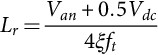
diLdt=Van+0.5VdcLr
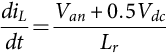
Since the slope of the inductor current (diL/dt) has to be smaller than the slope of the triangular waveform (λ) and the ripple current is defined, from Eqs. (41.37) and (41.38), as
Lr=Van+0.5Vdc4ξft
41.2.4.2 Design of the DC Capacitor
Transient changes in the instantaneous power absorbed by the load generate voltage fluctuations across the dc capacitor. The amplitude of these voltage fluctuations can be controlled effectively with an appropriate dc capacitor value. It must be noticed that the dc voltage control loop stabilizes the capacitor voltage after a few cycles, but is not fast enough to limit the first voltage variations. The capacitor value obtained with this criteria is bigger than the value obtained based on the maximum dc voltage ripple constraint. For this reason, the voltage across the dc capacitor presents a smaller harmonic distortion factor. The maximum overvoltage generated across the dc capacitor is given by
VCmax=1C∫θ2/ωθ1/ωiC(t)dt+Vdc
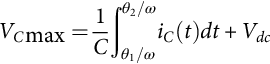
where VC max is the maximum voltage across the dc capacitor, Vdc is the steady-state dc voltage, and ic(t) is the instantaneous dc bus current. From Eq. (41.40),
C=1ΔV∫θ2/ωθ1/ωiC(t)dt
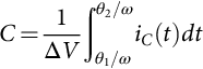
Eq. (41.41) defines the value of the dc capacitor, C, that will maintain the dc voltage fluctuation below ΔV p.u. The instantaneous value of the dc current is defined by the product of the inverter line currents with the respective switching functions. The mean value of the dc current that generates the maximum overvoltage can be estimated by
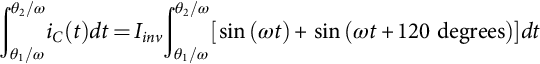
∫θ2/ωθ1/ωiC(t)dt=Iinv∫θ2/ωθ1/ω[sin(ωt)+sin(ωt+120degrees)]dt
In this expression, the inverter ac current is assumed to be sinusoidal. These operating conditions represent the worst case.
41.2.5 Technical Specifications
The standard specifications of shunt active power filters are the following:
• Number of phases: three phases and three wires or three phases and four wires (in case neutral currents need to be compensated)
• Input voltage: 200, 210, 220±10%![]() , 400, 420, 440±10%
, 400, 420, 440±10%![]() , 6600±10%
, 6600±10%![]()
• Frequency: 50/60 Hz±5%
• Number of restraint harmonic orders: 2nd–25th
• Harmonic restraint factor: 85% or more at the rated output
• Type of rating: continuous
• Response: 1 ms or less
For shunt active power filter, the harmonic restraint factor is defined as [1−(IH2/IH1)]×100%![]() , where IH1
, where IH1![]() is the harmonic currents flowing on the source side when no measure is taken for harmonic suppression and IH2
is the harmonic currents flowing on the source side when no measure is taken for harmonic suppression and IH2![]() is the harmonic currents flowing on the source side when harmonics are suppressed using an active filter.
is the harmonic currents flowing on the source side when harmonics are suppressed using an active filter.
41.3 Series Active Power Filters
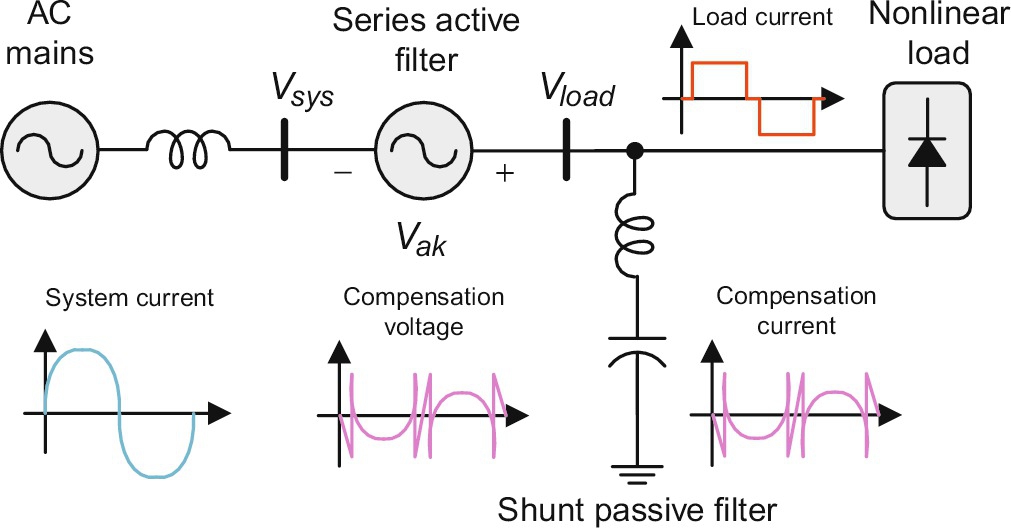
Series active power filters were introduced by the end of the 1980s [5] and operate mainly as a voltage regulator and harmonic isolator between the nonlinear load and the utility system. The series-connected active power filter is more preferable to protect the consumer from an inadequate supply voltage quality. This type of approach is specially recommended for the compensation of voltage unbalances, voltage distortion, and voltage sags from the ac supply and for low-power applications represents an economically attractive alternative to UPS, since no energy storage (battery) is necessary and the overall rating of the components is smaller. The series active power filter injects a voltage component in series with the supply voltage and therefore can be regarded as a controlled voltage source, compensating voltage sags and swells on the load side (Fig. 41.29).

If passive LC filters are connected in parallel to the load, the series active power filter operates as a harmonic isolator forcing the load current harmonics to circulate mainly through the passive filter rather than the power distribution system (hybrid topology) (Fig. 41.30). The main advantage of this scheme is that the rated power of the series active power filter is a small fraction of the load kilovolt-ampere rating, typically 5%. However, the rated apparent power of the series active power filter may increase, in case voltage compensation is required.
41.3.1 Power Circuit Structure
The topology of the series active power filter is shown in Fig. 41.31. In most cases, the power circuit configuration is based on a three-phase PWM voltage-source inverter connected in series with the power lines through three single-phase coupling transformers. For certain type of applications, the three-phase PWM voltage-source converter can be replaced by three single-phase PWM inverters. However, this type of approach requires more power components, which increases the cost.

In order to operate as a harmonic isolator, a parallel LC filter must be connected between the nonlinear loads and the coupling transformers (Fig. 41.30). Current harmonic and voltage compensation are achieved by generating the appropriate voltage waveforms with the three-phase PWM voltage-source inverter, which are reflected in the power system through three coupling transformers. With an adequate control scheme, series active power filters can compensate for current harmonics generated by nonlinear loads, voltage unbalances, voltage distortion, and voltage sags or swells at the load terminals. However, it is very difficult to compensate the load power factor with this type of topology. In four-wire power distribution systems, series active power filters with the power topology can also compensate the current harmonic components that circulate through the neutral conductor.
41.3.2 Principles of Operation
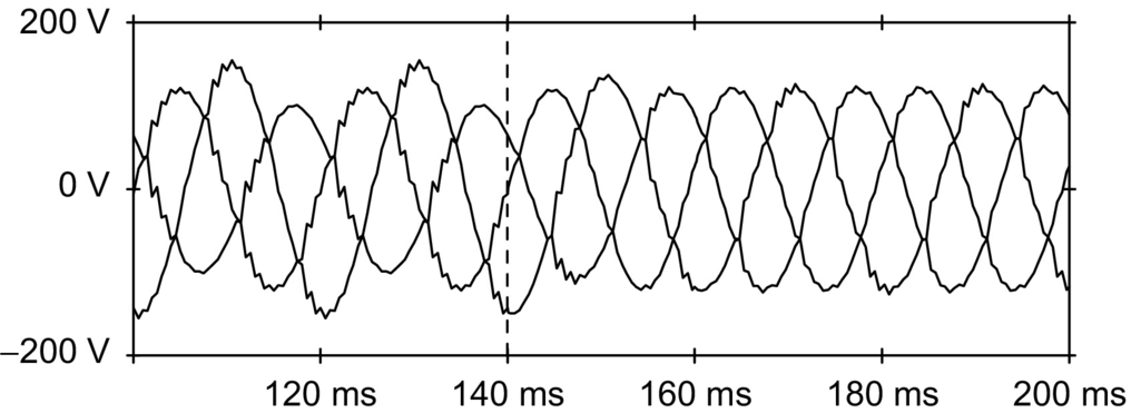
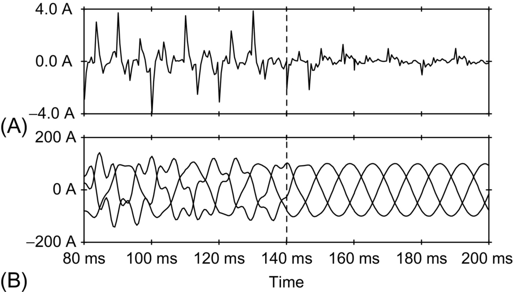
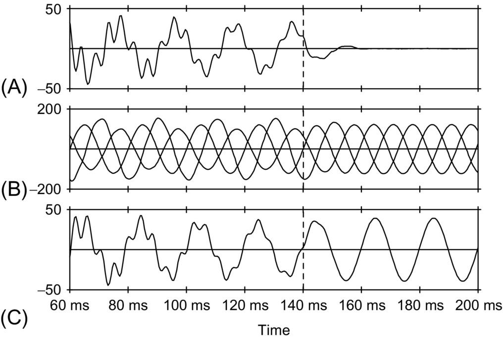
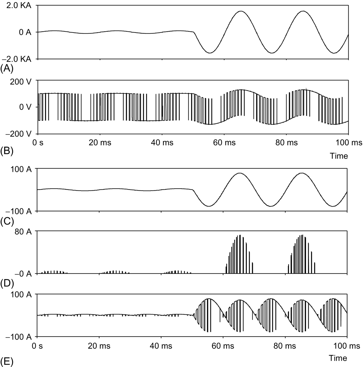
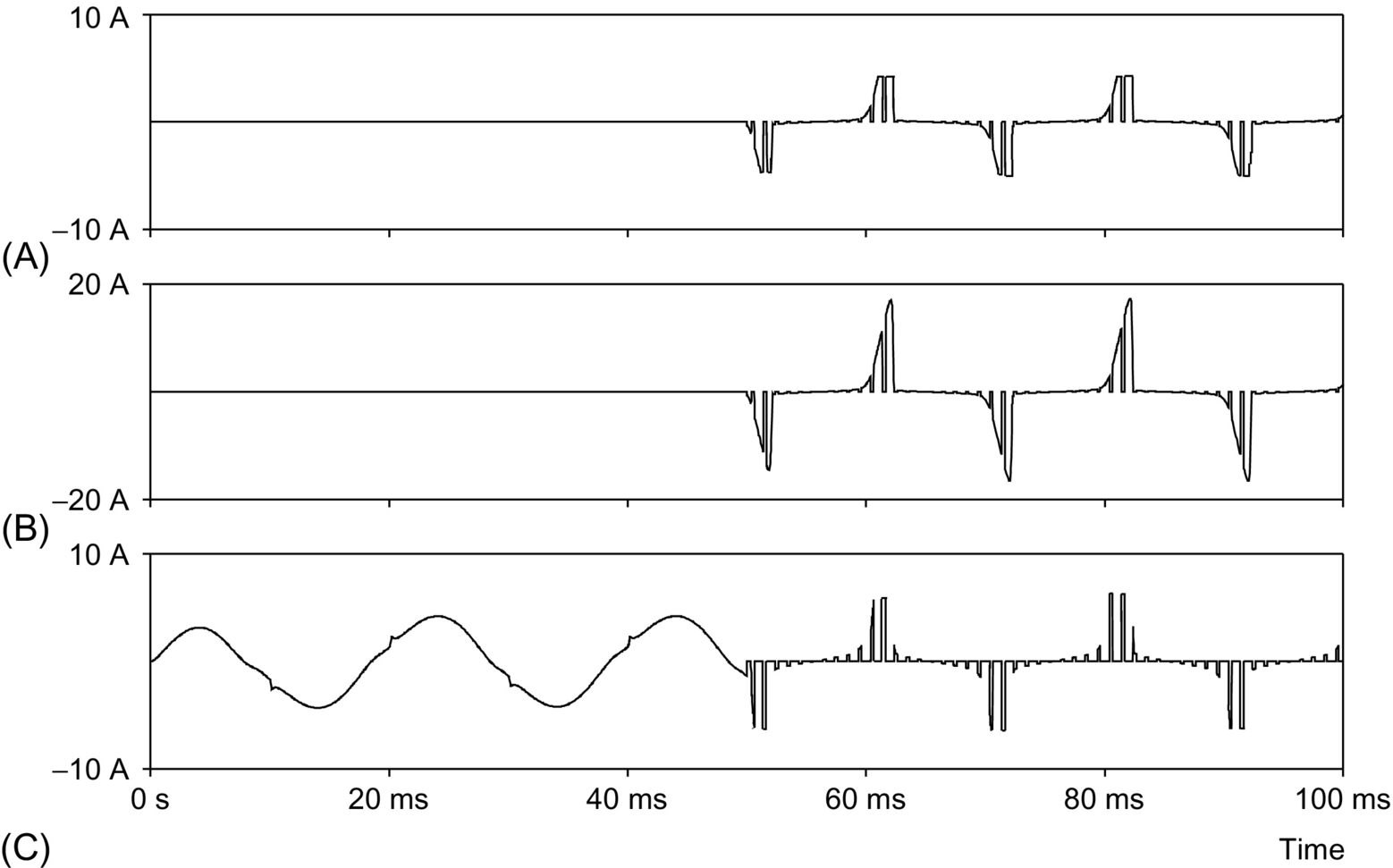
Series active power filters compensate current system distortion caused by nonlinear loads by imposing a high-impedance path to the current harmonics, which forces the high-frequency currents to flow through the LC passive filter connected in parallel to the load (Fig. 41.30). The high impedance imposed by the series active power filter is created by generating a voltage of the same frequency that the current harmonic component needs to be eliminated. Voltage regulation or voltage unbalance can be corrected by compensating the fundamental frequency positive, negative, and zero-sequence voltage components of the power distribution system (Fig. 41.29). In this case, the series active power filter injects a voltage component in series with the supply voltage and therefore can be regarded as a controlled voltage source, compensating voltage regulation on the load side (sags or swells) and voltage unbalance. Voltage injection of arbitrary phase with respect to the load current implies active power transfer capabilities that increases the rating of the series active power filter and in most cases requires an energy storage element connected in the dc bus. Voltage and current waveforms shown in Figs. 41.32–41.34 illustrate the compensation characteristics of a series active power filter operating with a shunt passive filter.
41.3.3 Power Circuit Design
The power circuit topology of the series active power filter is composed by the three-phase PWM voltage-source inverter, the second-order resonant LC filters, the coupling transformers, and the secondary ripple frequency filter (Fig. 41.30). The design characteristics for each of the power components are described below.
41.3.3.1 PWM Voltage-Source Inverter
Since series active power filter can compensate voltage unbalance and current harmonics simultaneously, the rated power of the PWM voltage-source inverter increases compared with other approaches that compensate only current harmonics, since voltage injection of arbitrary phase with respect to the load current implies active power transfer from the inverter to the system. Also, the transformer leakage inductance entails fundamental voltage drop and apparent power, which has to be supported by the inverter, reducing the series active filter inverter rating available for harmonic and voltage compensation. The rated apparent power required by the inverter can be obtained by calculating the apparent power generated in the primary of the coupling transformers. The voltage reflected across the primary winding of each coupling transformer is defined in Eq. (41.43):
Vseries=[K21{∑k≠1I2sk}1/2+K22{V2+V0}2]1/2
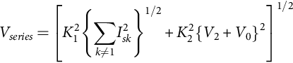
where Vseries is the root-mean-square voltage across the primary winding of the coupling transformer. Eq. (41.43) shows that the voltage across the primary winding of the transformer is defined by two terms. The first one is inversely proportional to the quality factor of the passive LC filter, while the second one depends on the voltage unbalance that needs to be compensated. K1 depends on the LC filter values, while K2 is equal to one. The current flowing through the primary winding of the coupling transformer, due to the harmonic currents (Eq. 41.44), can be obtained from the equivalent circuit shown in Fig. 41.35:
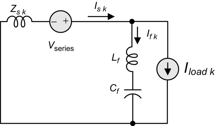
Isk=ZfkIlkZfk+Zsk+K1
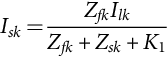
where Vseries=−K1Isk![]() . The fundamental component of the primary current depends on the amplitude of the negative- and zero-sequence component of the source voltage due to the system unbalance.
. The fundamental component of the primary current depends on the amplitude of the negative- and zero-sequence component of the source voltage due to the system unbalance.
41.3.3.2 Coupling Transformer
The purpose of the three coupling transformers is not only to isolate the PWM inverters from the source but also to match the voltage and current ratings of the PWM inverters with those of the power distribution system. The total apparent power required by each coupling transformer is one-third the total apparent power of the inverter. The turn ratio of the current transformer is specified according to the inverter dc bus voltage, K1 and Vref. The correct value of the turn ratio “a” must be specified according to the overall series active power filter performance. The turn ratio of the coupling transformer must be optimized through the simulation of the overall active power filter, since it depends on the values of different related parameters. In general, the transformer turn ratio must be high in order to reduce the amplitude of the inverter output current and to reduce the voltage induced across the primary winding. Also, the selection of the transformer turn ratio influences the performance of the ripple filter connected at the output of the PWM inverter. Taking into consideration all these factors, in general, the transformer turn ratio is selected equal to 1:20.
41.3.3.3 Secondary Ripple Filter
The design of the ripple filter connected in parallel to the secondary winding of the coupling transformer is performed following the method presented by Akagi in [6]. However, it is important to notice that the design of the secondary ripple filter depends mainly on the coupling transformer turn ratio and the current modulator used to generate the inverter gating signals. If the triangular carrier is used, the frequency of the triangular waveform has to be considered in the design of the ripple filter. The ripple filter connected at the output of the inverter avoids the induction of the high-frequency ripple voltage generated by the PWM inverter switching pattern at the terminals of the primary winding of the coupling transformer. In this way, the voltage applied in series to the power system corresponds to the components required to compensate voltage unbalanced and current harmonics. The single-phase equivalent circuit is shown in Fig. 41.36.
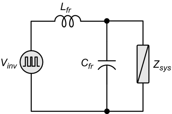
The voltage reflected in the primary winding of the coupling transformer has the same waveform as that of the voltage across the filter capacitor. For low-frequency components, the inverter output voltage must be almost equal to the voltage across Cfr. However, for high-frequency components, most of the inverter output voltage must drop across Lfr, in which case the voltage at the capacitor terminals is almost zero. Moreover, Cfr and Lfr must be selected in order not to exceed the burden of the coupling transformer. The ripple filter must be designed for the carrier frequency of the PWM voltage-source inverter. To calculate Cfr and Lfr, the system equivalent impedance at the carrier frequency, Zsys, reflected in the secondary must be known. This impedance is equal to
Zsys(secondary)=a2⋅Zsys(primary)
For the carrier frequency, the following design criteria must be satisfied:
| (i) XCfr≪XLfr |
to ensure that at the carrier frequency most of the inverter output voltage will drop across Lfr |
| (ii) XCfr and XLfr≪Zsys |
to ensure that the voltage divider is between Lfr and Cfr |
The small-rated LC passive filter exhibits a high-quality-factor circuit because of the high impedance on the output side. Oscillation between the small-rated inductor and capacitor may occur, causing undesirable high-frequency voltage across the ripple filter capacitor, which is reflected in the primary winding of the coupling transformer generating high-frequency current to flow through the power distribution system. It is important to note that this oscillation is very difficult to eliminate through the design and selection of the Lfr and Cfr values. However, it can be eliminated with the addition of a new control loop. The cause of the output voltage oscillation is explained with the help of Fig. 41.37. The transfer function Gp(s) between the input voltage Vi(s) and the output voltage VC(s) is given by the following equation:

Gp(s)=ω2ns2+2ξωns+ω2n

where ωn=√1/LfrCfr![]() and ξ=rL/2√Cfr/Lfr
and ξ=rL/2√Cfr/Lfr![]() .
.
Normally, the damping factor ξ is smaller than one, causing the voltage oscillation across the capacitor ripple filter, Cfr. Generally, relatively low impedance loads are connected to the output terminals of voltage-source PWM inverters. In these cases, the quality factor of the LC filter can be low, and the oscillation between the inductor Lfr and the capacitor Cfr is avoided [7].
41.3.3.4 Passive Filters
Passive filters connected between the nonlinear load and the series active power filter play an important role in the compensation of the load current harmonics. With the connection of the passive filters, the series active power filter operates as a harmonic isolator. The harmonic isolation feature reduces the need for precise tuning of the passive filters and allows their design to be insensitive to the system impedance and eliminates the possibility of filter overloading due to supply voltage harmonics. The passive filter can be tuned to the dominant load current harmonic and can be designed to correct the load displacement power factor.
However, for industrial loads connected to stiff supply, it is difficult to design passive filters that can absorb a significant part of the load harmonic current, and therefore, its effectiveness deteriorates. Specially, for compensation of diode rectifier type of loads, where a small kilovolt-ampere passive filter is required, it is difficult to achieve the required tuning to absorb significant percentage of the load harmonic currents. For this type of application, the passive filter cannot be tuned exactly to the harmonic frequencies because they can be overloaded due to the system voltage distortion and/or system current harmonics.
The single-phase equivalent circuit of a passive LC filter connected in parallel to a nonlinear current source and to the power distribution system is shown in Fig. 41.38. From this figure, the design procedure of this filter can be derived. The harmonic current component flowing through the passive filter ifh and the current component flowing through the source ish are given by the following expressions:

ifh=ZsZs+Zfih;ish=ZfZs+Zfih

At the resonant frequency, the inductive reactance of the passive filter is equal to the capacitive reactance of the filter, that is,
2πfrL=12πfrC
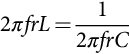
Therefore, the resonant frequency of the passive filter is equal to
fr=12π√LC

The passive filter bandwidth is defined by the upper and lower cutoff frequency, at which values the filter current gain is −3 dB, as shown in Fig. 41.39.
The magnitude of the passive filter impedance as a function of the frequency is shown in Fig. 41.40.

At the resonant frequency, the passive filter magnitude is equal to the resistance. If the resistance is zero, the filter is in short circuit. The quality factor of the passive filter is defined by the following expression:
Q=ωnLR

It is important to note that the operation of the series active power filter with off-tuned passive filter has an adverse impact on the inverter power rating compared with the normal case. The more off-tuned the passive filter, the more rated apparent power is required by the series active power filter.
41.3.3.5 Protection Requirements
Short circuits in the power distribution system generate large currents that flow through the power lines until the circuit breaker operates clearing the fault. The total clearing time of a short circuit depends on the time delay imposed by the protection system. The clearing time cannot be instantaneous due to the operating time imposed by the overcurrent relay and by the total interruption time of the power circuit breaker. Although power system equipment, such us power transformers and cables, are designed to withstand short-circuit currents during at least 30 cycles, the active power filter may suffer severe damage during this short time. The withstand capability of the series active power filter depends mainly on the inverter power semiconductor characteristics.
Since the most important feature of series active power filters is the small-rated power required to compensate the power system, typically 10%–15% of the load rated apparent power, the inverter semiconductors are rated for low values of blocking voltages and continuous currents. This makes series active power filters more vulnerable to power system faults.
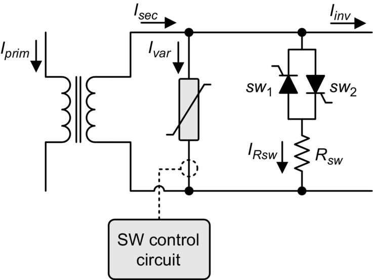
The block diagram of the protection scheme described in this section is shown in Fig. 41.41. It consists of a varistor connected in parallel to the secondary winding of each coupling transformer and a couple of antiparallel thyristors [8]. A special circuit detects the current flowing through the varistors and generates the gating signals of the antiparallel thyristors. The protection circuit of the series active power filter must protect only the PWM voltage-source inverter connected to the secondary of the coupling transformers and must not interfere with the protection scheme of the power distribution system. Since the primary of the active power filter coupling transformers is connected in series to the power distribution system, they operate as current transformers, so that their secondary windings cannot operate in open circuit. For this reason, if a short circuit is detected in the power distribution system, the PWM voltage-source inverter cannot be disconnected from the secondary of the current transformer. Therefore, the protection scheme must be able to limit the amplitude of the currents and voltages generated in the secondary circuits. This task is performed by the varistors and by the magnetic saturation characteristic of the transformers.
The main advantages of the series active power filter protection scheme described in this section are the following:
(i) It is easy to implement and has a reduced cost.
(ii) It offers full protection against power distribution short-circuit currents.
(iii) It does not interfere with the power distribution system.
When short-circuit currents circulate through the power distribution system, the low saturation characteristic of the transformers increases the current ratio error and reduces the amplitude of the secondary currents. The larger secondary voltages induced by the primary short-circuit currents are clamped by the varistors, reducing the amplitude of the PWM voltage-source inverter currents. After a few cycles of duration of the short circuit, the PWM voltage-source inverter is bypassed through a couple of antiparallel thyristors, and at the same time, the gating signals applied to the PWM voltage-source inverter are removed. In this way, the PWM voltage-source inverter can be turned off. The principles of operation and the effectiveness of the protection scheme are shown in Fig. 41.42.
The secondary short-circuit currents will circulate through the antiparallel thyristors and the varistors until the fault is cleared by the protection equipment of the power distribution system.
By using the protection scheme described in this subsection, the voltage and currents reflected in the secondary of the coupling transformers are significantly reduced. When short-circuit currents circulate through the power distribution system, the low saturation characteristic of the coupling transformers increases the current ratio error and reduces the amplitude of the secondary voltages and currents. Moreover, the saturated high secondary voltages induced by the primary short-circuit currents are clamped by the varistors, reducing the amplitude of the PWM voltage-source inverter ac currents. Once the secondary current exceeds a predefined reference value, the PWM voltage-source inverter is bypassed through a couple of antiparallel thyristors, and then, the gating signals applied to the PWM voltage-source inverter are removed. The effectiveness of the protection scheme is shown in Fig. 41.43.
By increasing the current ratio error due to the magnetic saturation, the energy dissipated in the secondary of the coupling transformer is significantly reduced. The total energy dissipated in the varistor for the different protection conditions is shown in Fig. 41.44.

41.3.4 Control Issues
The block diagram of a series active power filter control scheme that compensates current harmonics and voltage unbalance simultaneously is shown in Fig. 41.45.
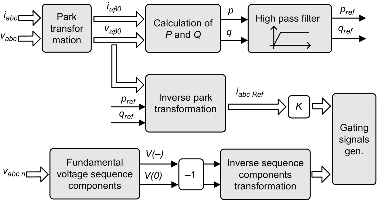
Current and voltage reference waveforms are obtained by using the Park transformation (instantaneous reactive power theory) voltage unbalance that is compensated by calculating the negative- and zero-sequence fundamental components of the system voltages. These voltage components are added to the source voltages through the coupling transformers compensating the voltage unbalance at the load terminals. In order to reduce the amplitude of the current flowing through the neutral conductor, the zero-sequence components of the line currents are calculated. In this way, it is not necessary to sense the current flowing through the neutral conductor.
41.3.4.1 Reference Signals Generator
The compensation characteristics of series active power filters are defined mainly by the algorithm used to generate the reference signals required by the control system. These reference signals must allow current and voltage compensation with minimum time delay. Also, it is important that the accuracy of the information contained in the reference signals allows the elimination of the current harmonics and voltage unbalance present in the power system. Since the voltage and current control schemes are independent, the equations used to calculate the voltage reference signals are the following:
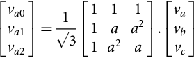
[va0va1va2]=1√3[1111aa21a2a].[vavbvc]
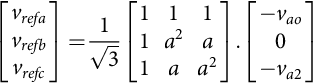
The voltages va, vb, and vc correspond to the power system phase-to-neutral voltages before the current transformer. The reference voltage signals are obtained by making the positive-sequence component, va1, zero and then applying the inverse of the Fortescue transformation. In this way, the series active power filter compensates only voltage unbalance and not voltage regulation. The reference signals for the voltage unbalance control scheme are obtained by applying the following equations:
[vrefavrefbvrefc]=1√3[1111a2a1aa2].[−vao0−va2]
In order to compensate current harmonics generated by the nonlinear loads, the following equations are used:
[iarefibreficref]=√23⋅[10−12√32−12−√32]⋅[vαvβ−vβvα]−1[prefqref]+1√3[i0i0i0]

where i0 is the fundamental zero-sequence component of the line current and is calculated using the Fortescue transformation Eq. (41.50):
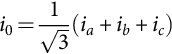
i0=1√3(ia+ib+ic)
In Eq. (41.40), pref, qref, vα, and vβ are defined according to the instantaneous reactive power theory. In order to avoid the compensation of the zero-sequence fundamental frequency current, the reference signal i0 must be forced to circulate through a high-pass filter generating a current i0′ that is used to create the reference signal required to compensate current harmonics. Finally, the general equation that defines the references of the PWM voltage-source inverter required to compensate voltage unbalance and current harmonics is the following:
[VrefaVrefbVrefc]=K1{√23[10-12√32-12-√32].[vαvβ-vβvα]-1[Prefqref]+1√3,[i′0i′0i′0]}+K2{1√3[1111a2a1aa2].[-va00-va2]}

where K1 is the gain of the coupling transformer that defines the magnitude of the impedance for high-frequency current components and K2 defines the degree of compensation for voltage unbalance, ideally K2 equals 1.
41.3.4.2 Gating Signals Generator
This circuit provides the gating signals of the three-phase PWM voltage-source inverter required to compensate voltage unbalance and current harmonic components. The current and voltage reference signals are added, and then, the amplitude of the resultant reference waveform is adjusted in order to increase the voltage utilization factor of the PWM inverter for steady-state operating conditions. The gating signals of the inverter are generated by comparing the resultant reference signal with a fixed-frequency triangular waveform. The triangular waveform helps to keep the inverter switching frequency constant (Fig. 41.46).
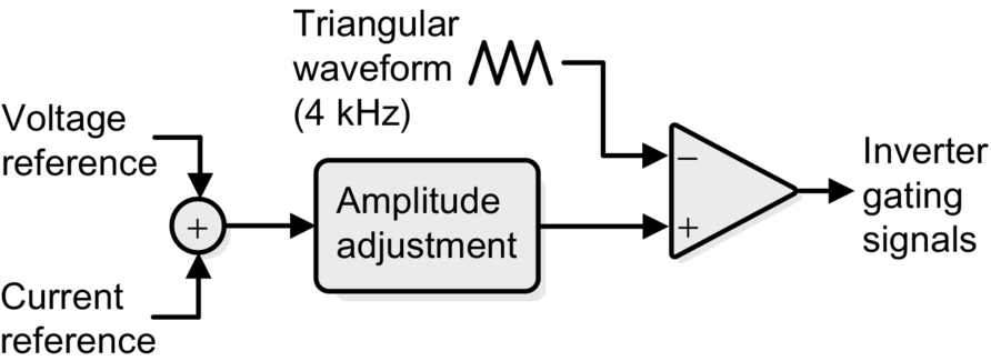
A higher voltage utilization of the inverter is obtained if the amplitude of the resultant reference signal is adjusted for the steady-state operating condition of the series active power filter. In this case, the reference current and reference voltage waveforms are smaller. If the amplitude is adjusted for transient operating conditions, the required reference signals will have a larger value, creating a higher dc voltage in the inverter and defining a lower voltage utilization factor for steady-state operating conditions. The inverter switching frequency must be higher in order not to interfere with the current harmonics that need to be compensated.
41.3.5 Control Circuit Implementation
Since the control scheme of the series active power filter must translate the current harmonic components that need to be compensated in voltage signals, a proportional controller is used. The use of a PI controller is not recommended since it would modify the reference waveform and generate new current harmonic components. The gain for proportional controller depends on the load characteristics, and its value fluctuates between one and two.
Another important element used in the control scheme is the filter that allows to generate pref and qref (Fig. 41.35). The frequency response of this filter is very important and must not introduce any phase shift or attenuation to the low-frequency harmonic components that must be compensated. A high-pass first-order filter tuned at 15 Hz is adequate. This corner frequency is required when single-phase nonlinear loads are compensated. In this case, the dominant current harmonic is the third. An example of the filter that can be used is shown in Fig. 41.47.
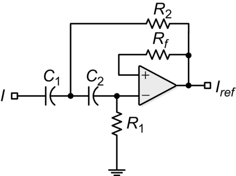
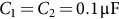 , R1=Rf=150kΩ
 , and R2=50kΩ
 ).
).The operator “a” required to calculate the sequence components of the system voltages (Fortescue transformation) can be obtained with the all-pass filter shown in Fig. 41.48.
The phase shift between Vo and Vi is given by the following expression:
θ=2arctan(2πfR2C)
Since the phase shift is negative, the operator “a” is obtained by using an inverter (180 degrees) and then by tuning θ=−60degrees![]() . The operator “a2” is obtained by phase shifting Vi by −120degrees
. The operator “a2” is obtained by phase shifting Vi by −120degrees![]() . Vi is synchronized with the system phase-to-neutral voltage Van.
. Vi is synchronized with the system phase-to-neutral voltage Van.
41.3.6 Experimental Results
The viability and effectiveness of series active power filters used to compensate current harmonics was proved in an experimental setup of 5 kVA. Current waveforms generated by a nonlinear load and using only passive filters and the combination of passive and the series active power filter are shown in Figs. 41.49 and 41.50.
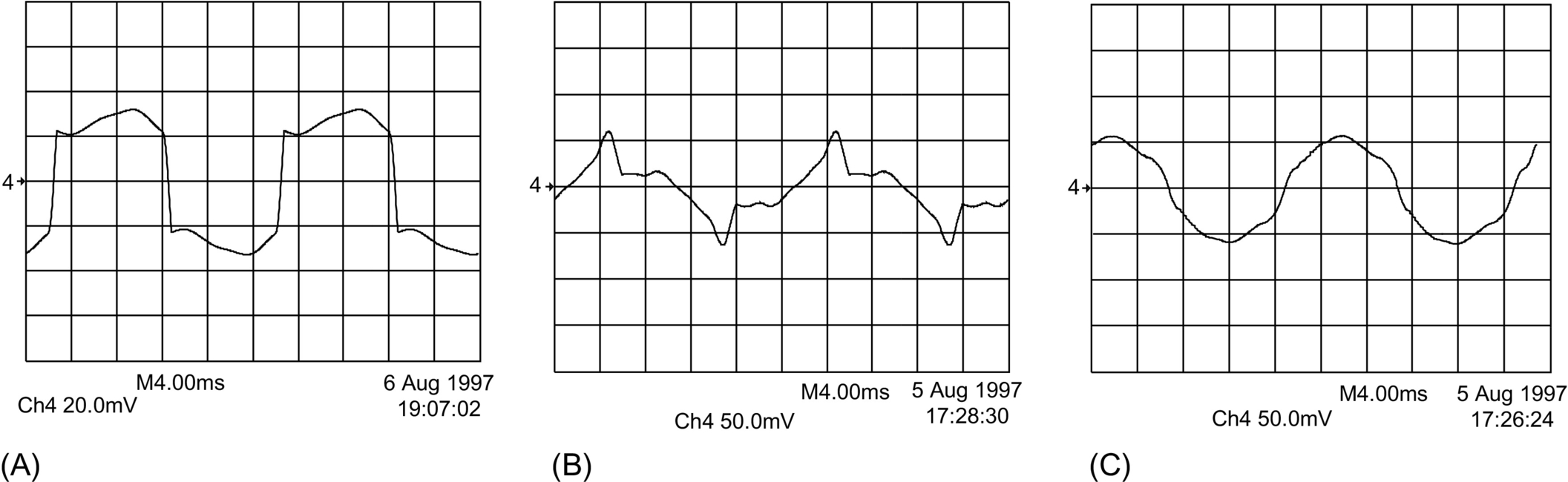
These figures show the effectiveness of the series active power filter, which reduces the overall THD of the current that flows through the power system from 28.9% (with the operation of only the passive filters) to 9% with the operation of the passive filters with the active power filter connected in series. The compensation of the current that flows through the neutral conductor is shown in Fig. 41.51.
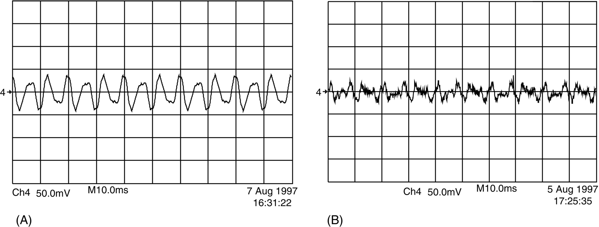
41.4 Hybrid Active Power Filters
Hybrid topologies composed of passive LC filters connected in series to an active power filter have already been proposed by the end of the 1980s [2,5,6,9,10]. Hybrid topology improves significantly the compensation characteristics of simple passive filters, making the use of active power filter available for high-power applications, at a relatively lower cost. Moreover, the compensation characteristics of already installed passive filters can be significantly improved by connecting a series active power filter at its terminals, giving more flexibility to the compensation scheme. Most of the technical disadvantages of passive filters described before can be effectively attenuate if an active power filter is connected in series to the passive approach as shown in Fig. 41.52.
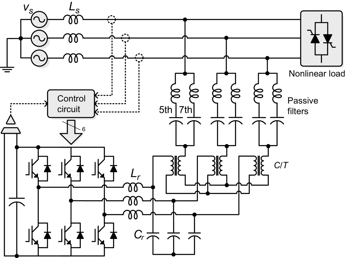
The hybrid active power filter topology is shown in Fig. 41.52. The active power filter is implemented with a three-phase PWM voltage-source inverter operating at fixed switching frequency and connected in series to the passive filter through a coupling transformer. Basically, the active power filter forces the utility line currents to become sinusoidal and in phase with the respective phase-to-neutral voltage, improving the compensation characteristics of the passive filter.
41.4.1 Principles of Operation
Since the active power filter is connected in series to the passive filter through a coupling transformer, it imposes a voltage signal at its primary terminals that forces the circulation of current harmonics through the passive filter, improving its compensation characteristics, independently of the variations in the selected resonant frequency of the passive filter. The block diagram of the proposed control scheme shown in Fig. 41.53 consists of three modules: the dc voltage control, the voltage reference generator, and the inverter gating signal generator.
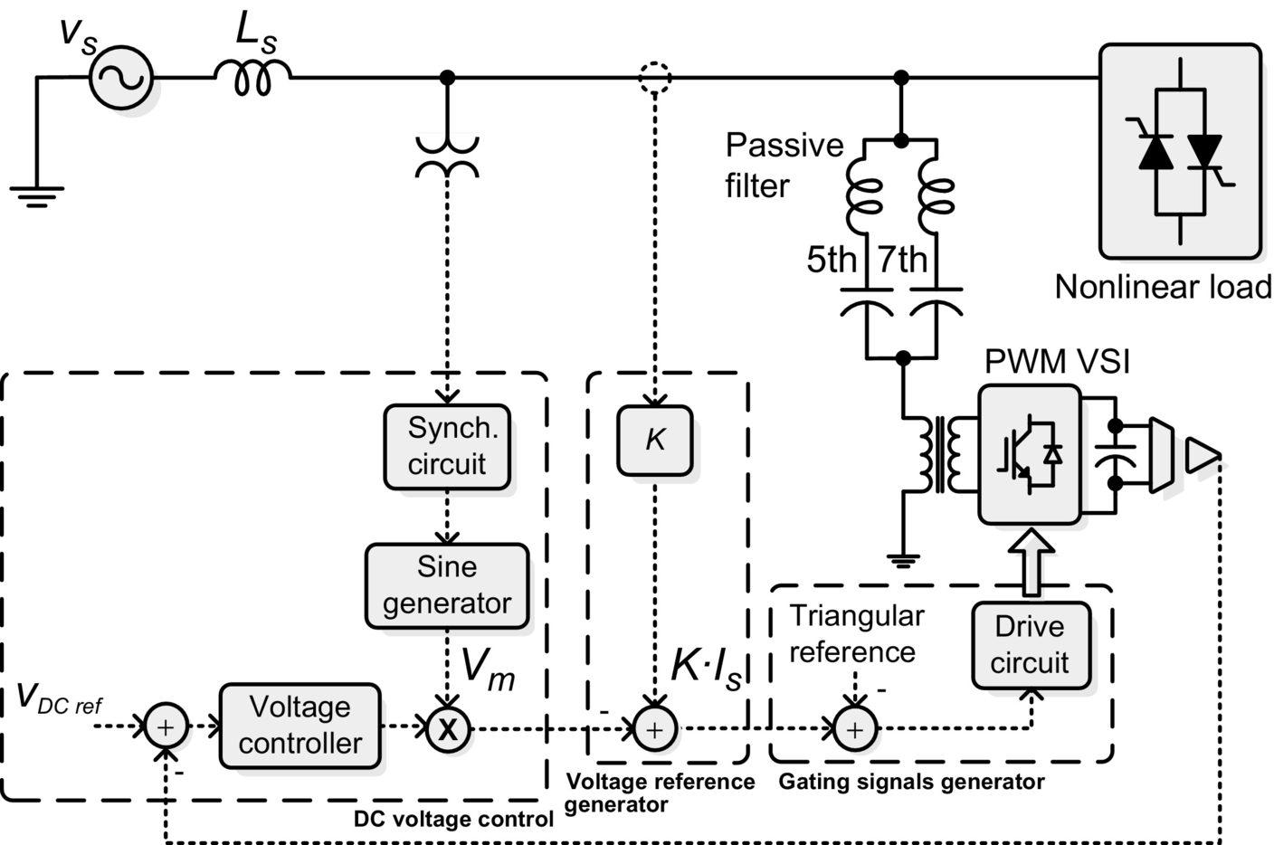
The voltage reference waveform required by the inverter control scheme is obtained by adjusting the amplitude of a sinusoidal reference waveform in phase with the respective phase-to-neutral voltage and then subtracting the respective ac line current (Fig. 41.53). The sinusoidal reference signal can be obtained from the voltage system (in case of low voltage distortion), or it can be generated from an EPROM synchronized with the respective phase-to-neutral voltage. The amplitude of this reference waveform controls the inverter dc voltage and the ac mains displacement power factor. The inverter dc voltage varies according with the amount of real power absorbed by the inverter, while the ac mains power factor depends on the amount of reactive power generated by the hybrid filter, which can be controlled by changing the amplitude of the fundamental component of the inverter output voltage.
The principles of operation for current harmonic and power factor compensation are explained with the help of the single-phase equivalent circuit shown in Fig. 41.54. In the current harmonic compensation mode, the active filter improves the filtering characteristic of the passive filter by imposing a voltage harmonic waveform at its terminals with an amplitude value equals to
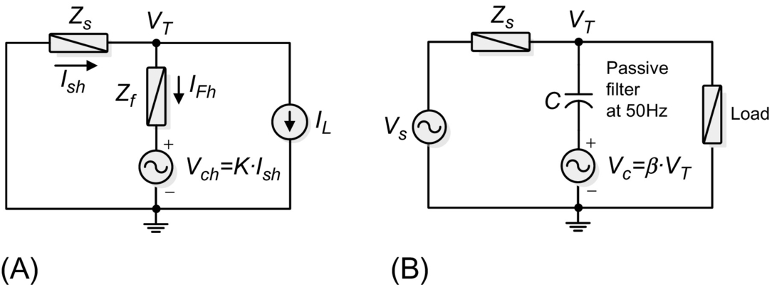
VCh=K⋅ISh
where ISh is the harmonic content of the line current to be compensated and K is the active power filter gain. If the ac mains voltage is purely sinusoidal, the ratio between the harmonic component of the nonlinear load current and the harmonic component of the ac line current (attenuation factor) is obtained from Fig. 41.54A and is equal to
IShILh=ZFK+ZF+ZS
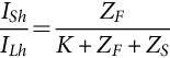
Eq. (41.58) shows that the filtering characteristics of the hybrid topology (ISh/ILh) depend on the value of the passive filter equivalent impedance, ZF. Moreover, since the tuned factor, δ, and the quality factor, Q, can modify the filter bandwidth and the passive filter harmonic equivalent impedance (Fig. 41.55), their values must be carefully selected in order to maintain the compensation effectiveness of the hybrid topology. In particular, a high value of the quality factor, Q, defines a large bandwidth of the passive filter, improving the compensation characteristics of the hybrid topology. On the other hand, a low value in the quality factor and/or a large value in the tuned factor increases the required voltage generated by the active power filter necessary to keep the same compensation effectiveness, which increases the active power filter rated power.
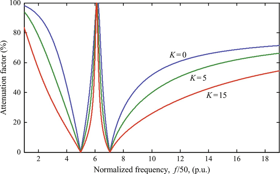
Fig. 41.55 shows how the active power filter gain, K, in Eq. (41.57) affects the harmonic attenuation factor of the line currents. The attenuation factor of the line current harmonics expressed in percentage is obtained from Eq. (41.59) and is shown in Fig. 41.56, for a power distribution system with two passive filters tuned at fifth and seventh harmonics.
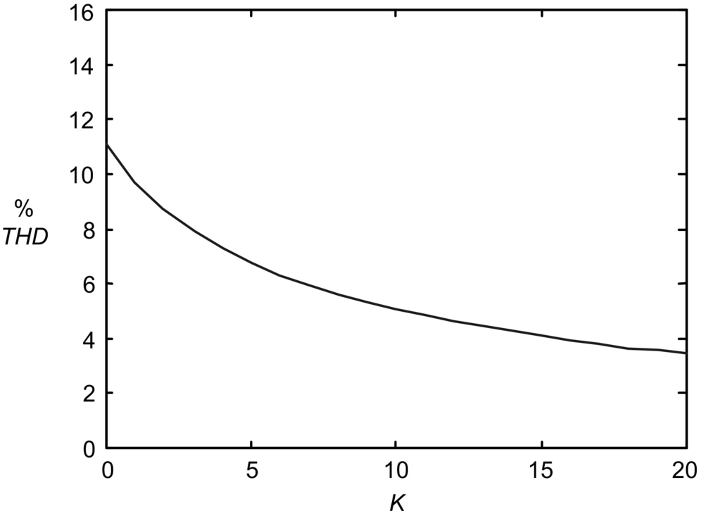
THDi=√∑h=2[ILh⋅(ZF/(ZS+ZF+K))]2IS1
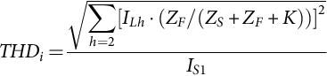
Eq. (41.59) indicates that the total harmonic distortion of the line current decreases if K increases. In other words, a better hybrid filter compensation is obtained for larger values of voltage harmonic components generated by the active power filter. Also, it is shown that the compensation capability of the hybrid filter depends on the compensation characteristic of the passive filter, that is, the filter impedance value and tuned frequency will affect the active filter rated power required to satisfy the system line current compensation requirements.
Displacement power factor correction can be achieved by controlling the voltage drop across the passive filter capacitor. In order to do that, a voltage at fundamental frequency is generated at the inverter ac terminals, with an amplitude equals to
VC=β⋅VT
Displacement power factor control can be achieved since at fundamental frequency the passive filter equivalent impedance is capacitive. The reactive power generated by the passive filter is obtained by changing the voltage imposed by the active power filter across the passive filter capacitor terminals. The passive filter fundamental current component is defined by the following expression:
iF=Cddt(vT−βvT)=(1−β)CdvTdt=CγβdvTdt
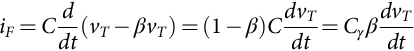
Eq. (41.61) proves that the equivalent capacitance at fundamental frequency Cγ can be modified by changing β. The reactive power generated by the active filter is β times the reactive power generated by the passive filter and can be defined by
Qγ=VC⋅IF=βVTIF
Eq. (41.62) shows that if β>0![]() , the active power filter generates a voltage at fundamental frequency in phase with VT, reducing the reactive power that flows to the load. If β<0
, the active power filter generates a voltage at fundamental frequency in phase with VT, reducing the reactive power that flows to the load. If β<0![]() , the active power filter generates a voltage at fundamental frequency phase shifted by 180 degrees with respect to VT, increasing the reactive power that flows to the load. In other words, by selecting a β positive or negative, the hybrid topology can generate or absorb reactive power at fundamental frequency, compensating for leading or lagging displacement power factor of the nonlinear load. This is achieved by changing the voltage across the passive filter capacitor CF.
, the active power filter generates a voltage at fundamental frequency phase shifted by 180 degrees with respect to VT, increasing the reactive power that flows to the load. In other words, by selecting a β positive or negative, the hybrid topology can generate or absorb reactive power at fundamental frequency, compensating for leading or lagging displacement power factor of the nonlinear load. This is achieved by changing the voltage across the passive filter capacitor CF.
41.4.2 The Hybrid Filter Compensation Performance
The design characteristics of the passive filters have an important influence on the compensation performance of the hybrid topology. The tuned frequency and quality factor of the passive filter directly influence the compensation characteristics of the hybrid topology. If these two factors are not properly selected, the rated power of the active filter must be increased in order to get the required compensation performance. The tuned factor, δ, in per unit with respect to the resonant frequency is defined by Eq. (41.63):
δ=ω−ωnωn
Here, δ defines the magnitude in which the passive filter resonant frequency changes due to the variations in the power system frequency and modifications in the values of the passive filter parameters L and C. The values of L and C can change due to aging conditions, temperature, or design tolerances. The tuning factor, δ, can also be defined as
δ=Δffn+12(ΔLLn+ΔCCn)
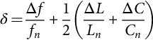
The quality factor, Q, of the passive filter is defined by Eq. (41.65):
Q=X0R

where X0 is equal to
X0=ωnL=1ωnC=√LC
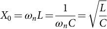
The passive filter quality factor, Q, defines the ratio between the passive filter reactance with respect to its resistance. In order to have a passive filter low impedance value in a limited frequency bandwidth, defined by the maximum expected changes of the rated power system frequency, it is necessary to reduce X0 or increase the passive filter resistance R, reducing the value of Q. However, if R increases, the equivalent impedance of the passive filter at the resonant frequency will increase, with the associated power losses, increasing the overall passive filter operational cost. On the other hand, the larger the value of Q, the lower is the passive filter equivalent impedance at the resonant frequency, increasing the currents harmonic components across the filter, at the resonant operating point.
41.4.2.1 Effects of the Power System Equivalent Impedance
The influence of the power system equivalent impedance on the hybrid filter compensation performance is related with its effects on the passive filter, since if the system equivalent impedance is lower than the passive filter equivalent impedance at the resonant frequency, most of the load current harmonics will flow mainly to the power distribution system. In order to compensate this negative effect on the hybrid filter compensation performance, K must be increased, as shown in Eq. (41.57), increasing the active power filter rated power.
Fig. 41.57 shows how the system equivalent impedance affects the relation between the system current THD with the active filter gain, K, in a power distribution system with passive filters tuned at the fifth and seventh harmonics. If Zs decreases, the current system THD increases, so in order to keep the same compensation performance of the hybrid scheme, the active power filter gain, K, must be increased. On the other hand, if Zs is high, it is not necessary to increase K in order to ensure a low THD value in the system current.
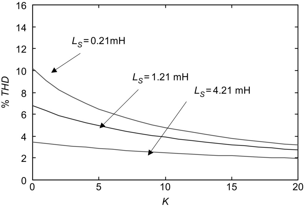
41.4.2.2 Effects of the Passive Filter Quality Factor
The quality factor, Q, defines the passive filter bandwidth. A passive filter with a high quality factor, Q, presents a larger bandwidth and better compensation characteristics. Eq. (41.67) defines the quality factor value in terms of the passive filter parameters L, R, and C. This equation shows that if R or C decreases, Q increases, and the filter bandwith becomes larger, improving the hybrid scheme compensation characteristics:
Q=1R√LC

Although by decreasing R or C the passive filter quality factor is improved, each element produces a different effect in the hybrid filtering behavior. For example, by increasing R, the filter equivalent impedance at the resonant frequency becomes bigger, affecting the current harmonic compensation characteristics at this specific frequency.
Fig. 41.58 illustrates how the system current THD changes with different values of C while keeping the filter tuned factor, δ, constant. It is important to note that the larger the value of C, the better is the compensation characteristic of the hybrid scheme. An appropriate value of C must be selected, since C cannot be increased too much. If C is too big, the fundamental component of the filter current will increase, overloading the hybrid filter and generating a large amount of reactive power to the power distribution system. A similar analysis is made for the value of the resistance, showing the results in Fig. 41.59.

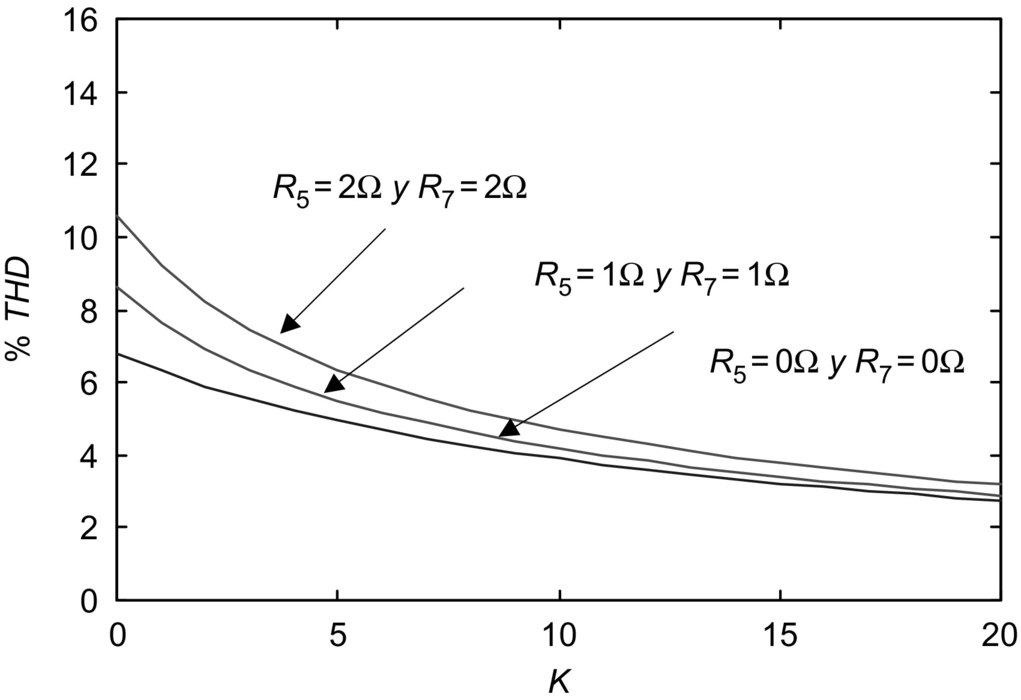
41.4.2.3 Effects of the Passive Filter Tuned Factor
The tuned factor, δ, is defined in Eq. (41.63). This factor affects the hybrid scheme performance especially at the passive filter resonant frequency, since δ defines the changes in the system frequency, affecting the value of the passive filter resonant frequency. Fig. 41.60 shows how the system current THD changes with respect to the active power filter gain, K, for different values of passive filter tuned factors. The larger the value of δ, the filtering performance of the hybrid filter becomes worst.
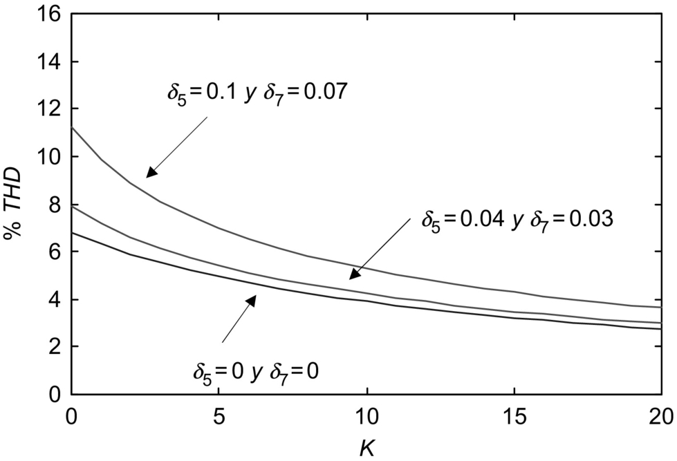
41.4.3 Experimental Results
A laboratory prototype using IGBT switches was implemented and tested in the compensation of a six-pulse controlled rectifier. The inverter was operated at 4 kHz switching frequency. Steady-state experimental results are illustrated in Figs. 41.61 and 41.62.
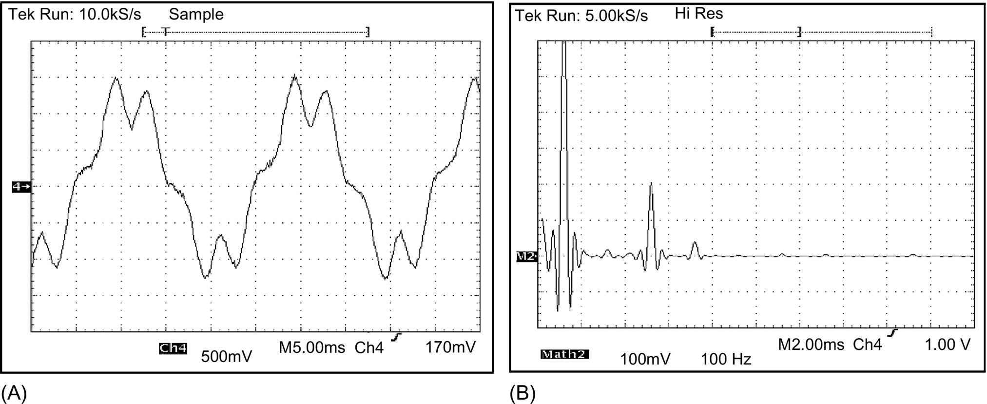
 ) and (B) line current frequency spectrum.
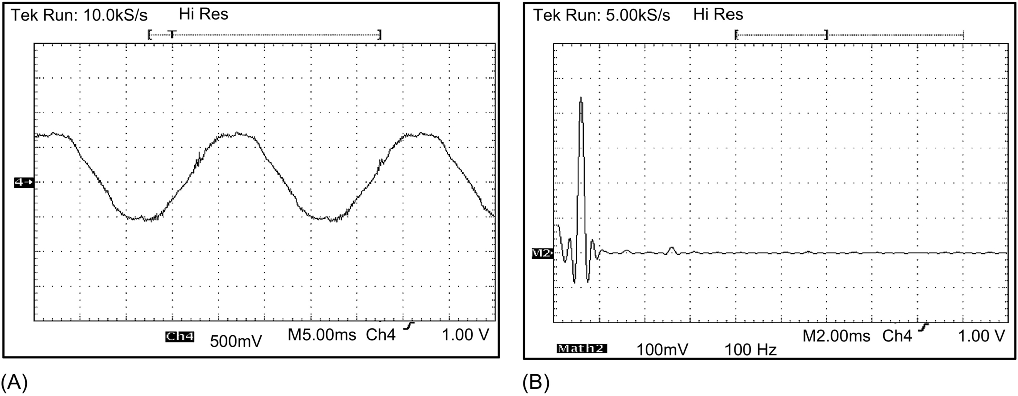
 ) and (B) associated frequency spectrum.
In case resonance is generated between the passive filter and system equivalent reactance, the system current THD increases to 60%. By connecting the active power filter, the line current THD is reduced to 4.9%, as shown in Figs. 41.63 and 41.64.
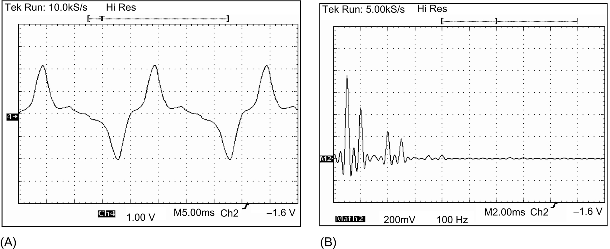
 ) and (B) associated frequency spectrum.
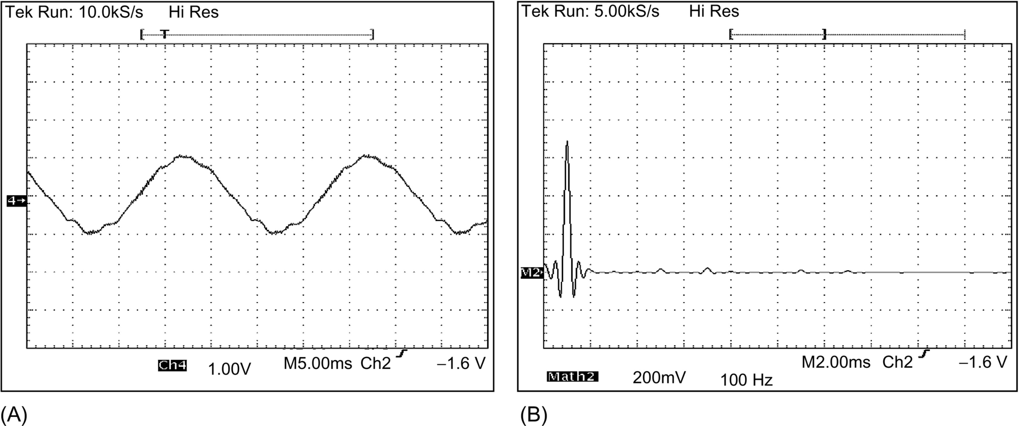
 ) and (B) associated frequency spectrum.
41.5 Predictive Control in Active Power Filters
Traditionally, active power filters have been controlled using pretuned controllers, such as PI-type or adaptive, for the current and for the dc voltage loops. PI controllers must be designed based on the equivalent linear model, while predictive controllers use the nonlinear model, which is closer to real operating conditions. Providing an accurate model is used, a predictive controller improves the performance of the active power filter, especially during transient operating conditions, because it can quickly follow the current reference signal while maintaining a constant dc voltage.
Fig. 41.65 shows the equivalent circuit of a shunt APF application. One advantage of using model-based predictive control in active power filter applications is that the power converter model and parameter are well-known or can be easily determined. These parameters are obtained from the converter output ripple filter (Zf) and the power system equivalent impedance (Zs). The former is known from the design stage of the active power filter, and the latter can be determined using well-known standard procedures of calculation or online estimation.
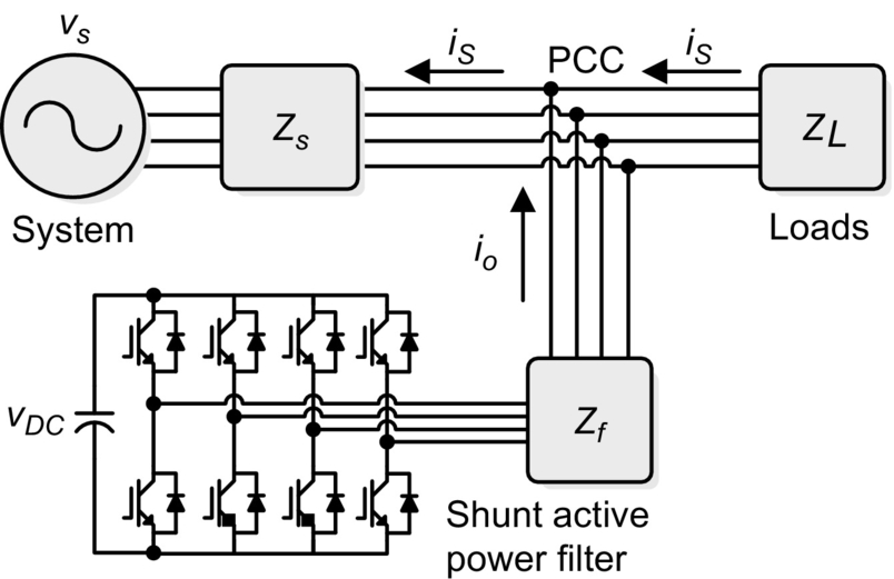
41.5.1 Predictive Current Control
The block diagram of the proposed digital predictive current control scheme is shown in Fig. 41.66. This control scheme entails an optimization algorithm that is implemented in a microprocessor. Consequently, the analysis has to be developed using discrete mathematics in order to consider additional restrictions such as time delays and approximations. The essence of model-based predictive control is the use of the model of the system to be controlled to predict the future state of some of its variables. The controller then, according to a predefined optimization criterion, selects the optimum switching pattern that has to be applied to the power converter in order for it to achieve the future state with minimum error. The predictive control algorithm can be implemented with three main blocks, as shown in Fig. 41.66.
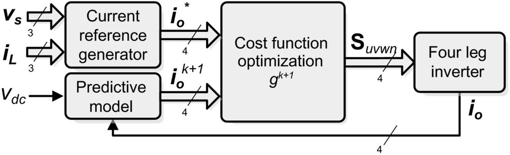
41.5.1.1 Current Reference Generator
This unit is designed to generate the required current reference that is used to compensate the undesirable load current components. In this case, the system voltages, the load currents, and the dc voltage converter are measured, while the neutral output current and neutral load current are generated directly from these signals.
41.5.1.2 Prediction Model
The converter model is used to predict the output converter current. Since the controller operates in discrete time, both the controller and the system model must be represented in a discrete-time domain. The discrete-time model consists of a recursive matrix equation that represents this prediction system. This means that for a given sampling time Ts, knowing the converter switching states and control variables at instant kTs, it is possible to predict the next states at any instant [k+1]Ts. Due to the first-order nature of the state equations that describe the model in (41.68) and (41.69), a sufficiently accurate first-order approximation of the derivative is considered:
vo=vxn−Reqio−Leqdiodt
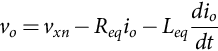
vxn=Sx−Snvdc,x=u,v,w,n.
Therefore, the 16 possible output current predicted values can be obtained from (41.68) as
io[k+1]=TsLeq(vxn[k]−vo[k])+(1−ReqTsLeq)io[k]
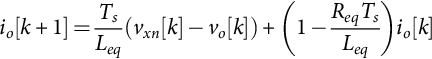
41.5.1.3 Cost Function
In order to select the optimal switching state that must be applied to the power converter, the 16 predicted values obtained for io[k+1] are compared with the reference using a cost function g, as follows:
g[k+1]=(i⁎ou[k+1]−iou[k+1])2+(i⁎ov[k+1]−iov[k+1])2+(i⁎ow[k+1]−iow[k+1])2+(i⁎on[k+1]−ion[k+1])2
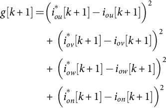
The output current (io) is equal to the reference (io⁎) when g=0. Therefore, the optimization goal of the cost function is to achieve a g-value close to zero. During each sampling state, the voltage vector vxn that minimizes the cost function is found and then applied to the converter in the next sampling state.
41.5.2 Current Reference Generator
A dq-based current reference generator scheme is used to obtain the active power filter current reference signals (see “Synchronous Reference Frame Algorithm” section). This scheme presents a fast and accurate signal-tracking capability. This characteristic avoids voltage fluctuations that deteriorate the current reference signal affecting compensation performance. The current reference signals are obtained from the corresponding load currents as shown in Fig. 41.67. The cutoff frequency of the LPF used in this example is 20 Hz.

The current that flows through the neutral of the load is compensated by injecting the same instantaneous value obtained from the phase currents but with a phase shift of 180 degrees as shown in (41.72):
i⁎on=−(iLu+iLv+iLw)
41.5.3 DC Voltage Control
The dc voltage converter is controlled with a traditional PI controller. This is an important issue in the evaluation, since the cost function (41.71) is designed using only current references, in order to avoid the use of weighting factors. Generally, these weighting factors are obtained experimentally, and they are not well defined when different operating conditions are required. Additionally, the slow dynamic response of the voltage across the electrolytic capacitor does not affect the current transient response. For this reason, the PI controller represents a simple and effective alternative for the dc voltage control.
The dc voltage remains constant (with a minimum value of √6vs(rms)) until the active power absorbed by the converter decreases to a level where it is unable to compensate for its losses. The active power absorbed by the converter is controlled by adjusting the amplitude of the active power reference signal ie, which is in phase with each phase voltage. The equivalent closed-loop transfer function of the given system with a PI controller is
vdcie=ω2na(s+a)s2+2ζωns+ω2n

Since the time response of the dc voltage control loop does not need to be fast, a damping factor ζ=1 and a natural angular speed ωn=2π100 rad/s are used to obtain a critically damped response with minimal voltage oscillation. The corresponding integral time Ti=1/a and proportional gain Kp can be calculated as
ζ=√38KPvs√2TiCdcv⁎dc
ωn=√32KPvs√2Cdcv⁎dcTi
41.5.4 Performance Evaluation
The compensation effectiveness of the active power filter is corroborated in a 2 kVA experimental setup. In order to verify the effectiveness of the current harmonic compensation, a six-pulse rectifier was selected as a nonlinear load. A step load change was applied to evaluate the transient response of the dc voltage loop. Finally, an unbalanced load was used to validate the performance of the neutral current compensation. The proposed predictive control algorithm was programmed using an S-function block that allows simulation of a discrete model that can be easily implemented in a real-time interface (RTI) on the dSPACE DS1103 R&D control board. The complete control loop is executed by the controller every 20 μs, while the selected switching state is available at 16 μs. An average switching frequency of 4.64 kHz is obtained.
Fig. 41.68 shows the transient response of the compensation scheme. Fig. 41.68A shows that the line current becomes sinusoidal when the active power filter starts compensating and the dc voltage behaves as expected. Fig. 41.68B indicates that the total harmonic distortion of the line current (THDi) is reduced from 27.1% to 4.5%. This is a consequence of the good tracking characteristic of the current references, as shown in Fig. 41.68D.
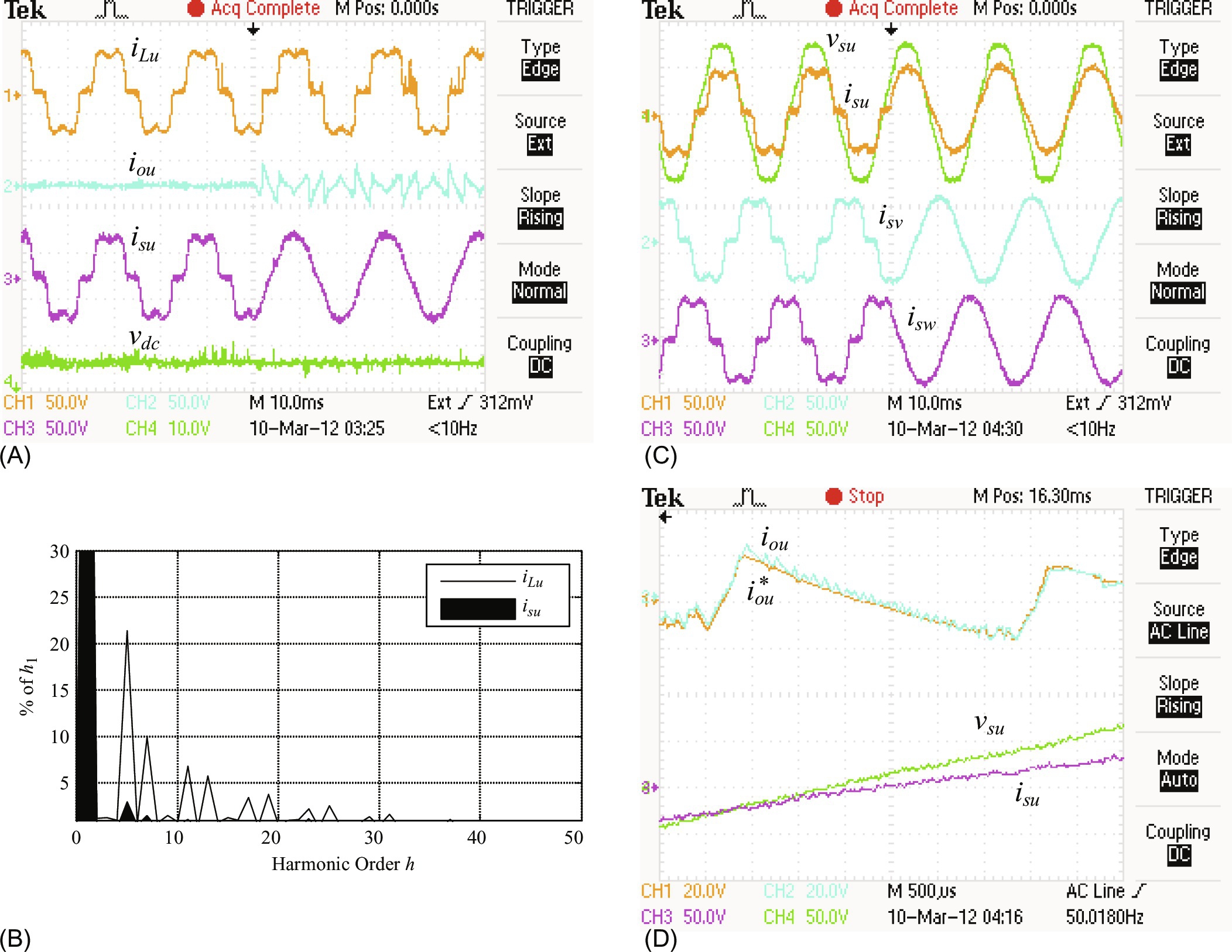
In Fig. 41.69, the transient response of the active power filter under a step load change is shown. In this case, a step load change is applied from 0.6 to 1.0 p.u. The line currents remain sinusoidal, and the dc voltage returns to its reference with a typical transient response of an underdamped second-order system (maximum overshoot of 5% and two grid cycles of settling time).
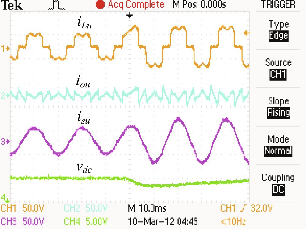
Finally, the load connected to phase u was increased from 1.0 to 1.3 p.u. The corresponding waveforms are shown in Fig. 41.70. Fig. 41.70A shows that the active filter is capable of compensating the current in the neutral conductor with a fast transient response. Moreover, Fig. 41.70B shows that the system neutral current ion is effectively compensated and eliminated and system currents remain balanced even if an 11% current imbalance is applied.
