2.2 PIC18F2410 Architecture
The pin configuration (DIP package) of the PIC18F2410 microcontroller is shown in Figure 2.2. As we shall see later, most of the pins are multiplexed and can be used for different purposes. For example, pin 2 is named as RA0/AN0 and this is the PORT A least significant port pin. This pin can be used as an analogue input (named AN0), or as a digital I/O (named RA0).
Figure 2.2 PIC18F2410 pin configuration (DIP package). (Reproduced with permission from Microchip Inc)
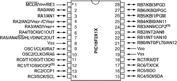
Figure 2.3 shows the simplified internal architecture of the PIC18F2410 microcontroller. The CPU is at the centre of the diagram and consists of an 8-bit ALU, an accumulator register (WREG), and an 8 × 8 multiplier module. The multiplier takes data from the accumulator register and the data bus, and provides the 16-bit result in registers PRODH and PRODL, where the result can be read through the data bus.
Figure 2.3 Internal architecture of the PIC18F2410 microcontroller. (Reproduced with permission from Microchip Inc)
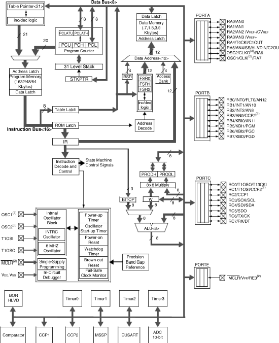
The program memory and the program counter are shown at the top left corner of the figure. The memory address consists of 21 bits, capable of addressing up to 2 MB of memory data, although here only 16 KB is used. The program counter consists of two 8-bit registers PCH and PCL, and a 5-bit register PCU. A 32-level deep stack can be seen at the bottom of the program counter. The stack is used to store the return addresses when a subroutine is called or when an interrupt occurs. The stack is independent of the data memory and is addressed with a 5-bit stack pointer STKPTR. The stack pointer is initialised to 00 000 after a reset.
The data memory can be seen at the top right corner of the figure. The data addresses are 12 bits, thus up to 4 KB data can be addressed, although here only 768 bytes of data memory are implemented.
The instruction decode and control logic, located at the centre of the figure, decodes the instructions fetched from the program memory and sends the appropriate control signals to all parts of the microcontroller to implement the required operation.
Just below the instruction decode and control logic, we see the timing and power control module. This module is responsible for generating the clock timing pulses for both the external and internal clock. In addition, this module controls the power-on timer, oscillator startup, POR, watchdog timer, brown-out reset, single-supply programming, in-circuit debugger, and the fail safe clock monitoring.
At the bottom of the figure we can see the four timer modules, comparator/capture/pwm modules, master synchronous serial port module (MSSP), USART module, and the A/D converter module.
There are 4 I/O ports named PORTA, PORTB, PORTC and PORTE, and 25 I/O pins shown at the right side of the figure. PORTA, PORTB and PORTC are 8-bit ports, while PORTE has only 1 bit. All ports pins are bi-directional when configured as digital I/O.
2.2.1 The Program Memory
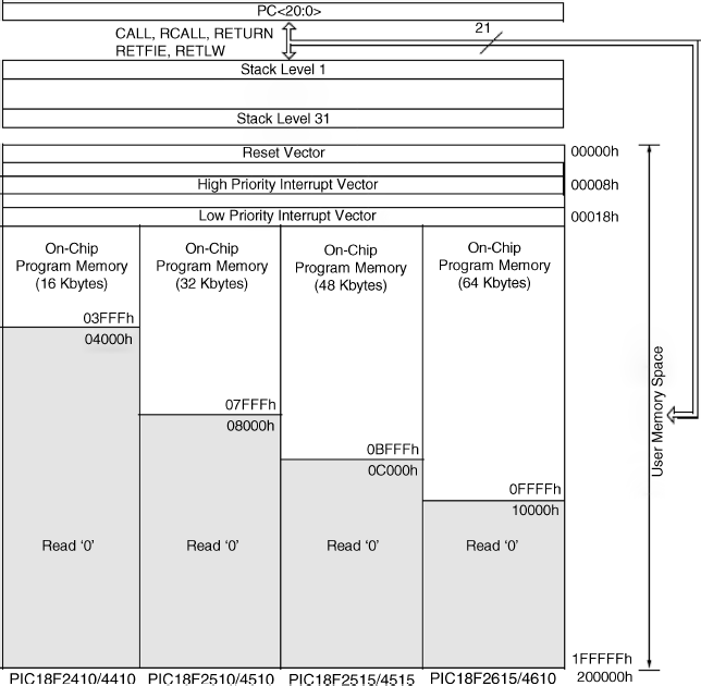
Figure 2.4 shows a memory map of the PIC18F2410 microcontroller. The device has a 21-bit program counter (PC <20: 0>), capable of addressing up to 2 MB of memory, although here only 16 KB is used, ranging from 00 000 h to 03 FFFh. Memory addresses above 0400 h are read as 0 and are not available. The Reset vector is at address 00 000 h and the program counter is loaded with this address after a reset, causing the program starting at this address to be executed. Addresses 00 008 h and 00 018 h are the high and low priority interrupt vectors, respectively. Thus, for example, when a low priority interrupt occurs, the program jumps to address 00 008 h.
Figure 2.4 Program memory map of the PIC18F2410 microcontroller. (Reproduced with permission from Microchip Inc)
An instruction cycle in an 8-bit PIC microcontroller consists of 4 cycles (Q1 to Q4). A fetch cycle begins with the program counter incrementing in Q1. The fetched instruction is decoded and executed in cycles Q2, Q3 and Q4. A data memory location is read during the Q2 cycle and written during the Q4 cycle. Because an instruction cycle consists of 4 cycles, the performance of a PIC microcontroller is measured by dividing the operating clock frequency by 4. For example, a processor operating with a 40 MHz clock frequency has a MIPS (Million Instructions Per Second) rating of 10 MIPS.
2.2.2 The Data Memory
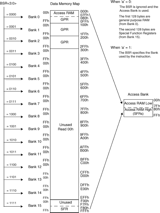
Figure 2.5 shows the data memory of the PIC18F2410 microcontroller. Data memory is addressed with 12 bits, capable of addressing up to 4 KB of memory. The memory is usually divided into 16 banks, each bank 256 bytes long. The PIC18F2410 microcontroller uses only the first 3 banks (BANK 0, BANK 1 and BANK 2) from address 000 h to 2 FFh. The remaining banks, except half of BANK 15, are not used and return 0 when accessed. The upper part of BANK 15 is reserved for the SFR (Special Function Registers) registers. SFR registers control internal modules of the microcontrollers, such as A/D converter, interrupts, timers, USART, I/O ports, and so on.
Figure 2.5 Data memory map of the PIC18F2410 microcontroller. (Reproduced with permission from Microchip Inc)
2.2.3 Power Supply Requirements
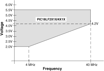
The PIC18F2410 microcontroller operates with a power supply of 4.2 to 5.5 V, at the full speed of 40 MHz. The low-power version of the microcontroller (PIC18LF2410) can operate at a voltage as low as 2.0 V. As shown in Figure 2.6, at low voltages the maximum operating frequency is limited. For example, at 2.0 V the maximum operating frequency should not exceed 4 MHz. In practical applications, most microcontrollers are operated with a supply of 5.0 V, derived using a 78L05/7805 or a similar voltage regulator.
Figure 2.6 Power supply requirements. (Reproduced with permission from Microchip Inc)
2.2.4 Oscillator Configurations
The PIC18F2410 microcontroller can be operated in 10 different oscillator modes. The user can program the required oscillator mode during programming of the device. These modes are:
- low-power crystal (LP);
- Crystal/Resonator (XT);
- high-speed crystal/resonator with PLL enabled (HSPLL);
- external resistor-capacitor with Fosc/4 on OSC2 (RC);
- external resistor-capacitor with I/O on OSC2 (RCIO);
- internal oscillator with Fosc/4 on OSC2 and I/O on OSC1 (INTIO1);
- internal oscillator with I/O on OSC2 and OSC1 (INTIO2);
- external clock with Fosc/4 output on OSC2(EC);
- external clock with I/O on OSC2 (ECIO).
2.2.4.1 Using Crystal (LP/XT)
A crystal should be used in applications requiring high timing accuracies. The crystal is connected to pins OSC1 and OSC2 of the microcontroller with a pair of capacitors, as shown in Figure 2.7. That capacitor value depends on the oscillator mode and is shown in Table 2.2. In most applications, a 15–33 pF capacitor should be sufficient to achieve stability.
Figure 2.7 Operation with a crystal
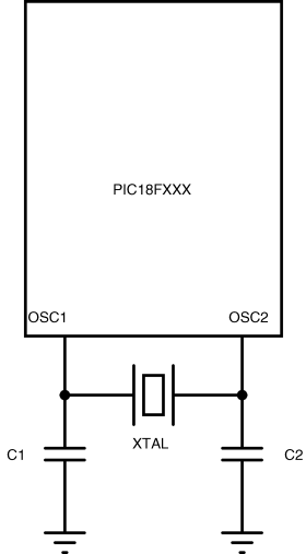
Table 2.2 Required capacitor values.
| Mode | Frequency | C1,C2 (pF) |
| LP | 32 kHz | 33 |
| 200 kHz | 15 | |
| XT | 200 kHz | 22–68 |
| 1.0 MHz | 15 | |
| 4.0 MHz | 15 | |
| HS | 4.0 MHz | 15 |
| 8.0 MHz | 15–33 | |
| 20.0 MHz | 15–33 | |
| 25.0 MHz | 15–33 |
2.2.4.2 Using Resonator (XT)
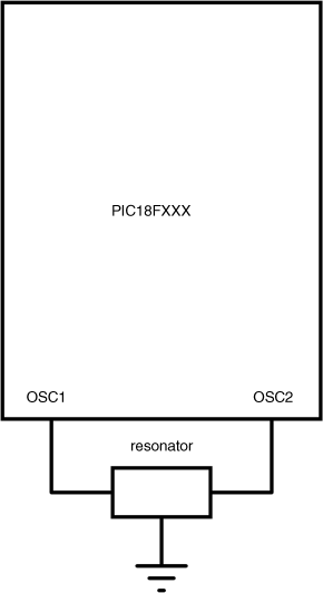
A resonator should be used in low-cost applications where high timing accuracy is not essential. Resonators are available at low to medium frequencies, up to 10 MHz. The resonator should be connected to pins OSC1 and OSC2 of the microcontroller, as shown in Figure 2.8.
Figure 2.8 Operation with a resonator
2.2.4.3 Using External Resistor-Capacitor (RC/RCIO)
Using an external resistor-capacitor (RC) for timing provides the cheapest solution. Here, the clock frequency depends on the chosen resistor and capacitor values, component tolerances, power supply, temperature, and ageing of components. The clock frequency is not accurate and can easily change from unit to unit due to component tolerances.
Table 2.3 gives the approximate clock frequency with different RC combinations. The resistor should be between 3 K and 100 K, and the capacitor should be greater than 20 pF. The clock frequency is given approximately by
(2.1) ![]()
Table 2.3 Selecting a resistor and capacitor.
| C (pF) | R (K) | Frequency (MHz) |
| 22 | 3.3 | 3.3 |
| 4.7 | 2.3 | |
| 10.0 | 1.08 | |
| 30 | 3.3 | 2.4 |
| 4.7 | 1.7 | |
| 10.0 | 0.793 |
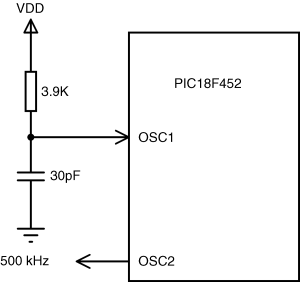
As an example, for a 2 MHz clock, we can choose a capacitor of 30 pF and a resistor of 3.9 K. Figure 2.9 shows the circuit diagram for RC mode operating at approximately 2 MHz. Notice that in RC mode, a clock is output from pin OSC2 with a frequency of Fosc/4, that is 500 Hz in this example.
Figure 2.9 Operation with a resistor-capacitor
The RCIO mode is similar to the RC mode, except that in RCIO mode the OSC2 pin is available as a general purpose I/O.
2.2.4.4 Using the Internal Oscillator (INTIO1/INTIO2)
An internal oscillator can be extremely useful in many applications. First, it eliminates the need to use an external timing device, thus reducing the cost and the component count. Second, by using an internal oscillator, the microcontroller oscillator pins become available for general purpose I/O.
PIC18F2410 includes two internal oscillators. A factory calibrated 8 MHz clock source (IINTOSC), and an RC based 31 kHz clock source (INTRC). In the INTIO1 mode, the OSC2 pin outputs a clock at frequency Fosc/4, while the OSC1 pin (RA7) can be used as general digital I/O. In the INTIO2 mode, both OSC1 and OSC2 pins function as general purpose I/O pins (RA6 and RA7).
Although the 8 MHz clock source is factory calibrated, the frequency can drift slightly and the SFR register OSCTUNE can be used to re-calibrate this clock source (see manufacturers' data sheet for more information). The 8 MHz clock drives a postscaler, and a multiplexer is used to provide clock frequencies in the range 31 kHz to 8 MHz.
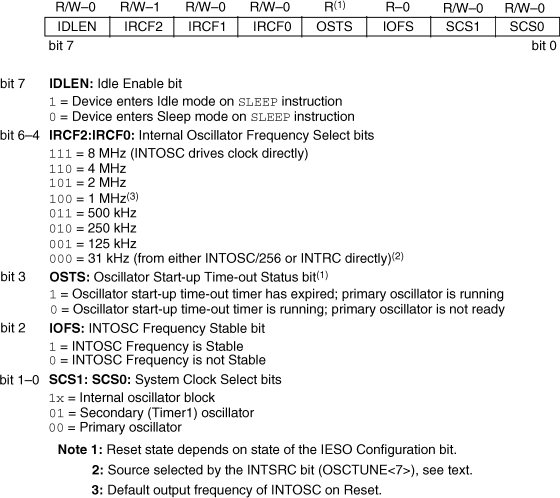
Figure 2.10 shows the internal structure of the clock selection mechanism. SFR register OSCCON controls the clock selection, as shown in Figure 2.11. For example, to select an 4 MHz internal clock, bits <6: 4> of OSSCON should be set to binary pattern ‘110’.
Figure 2.10 Clock selection mechanism. (Reproduced with permission from Microchip Inc)
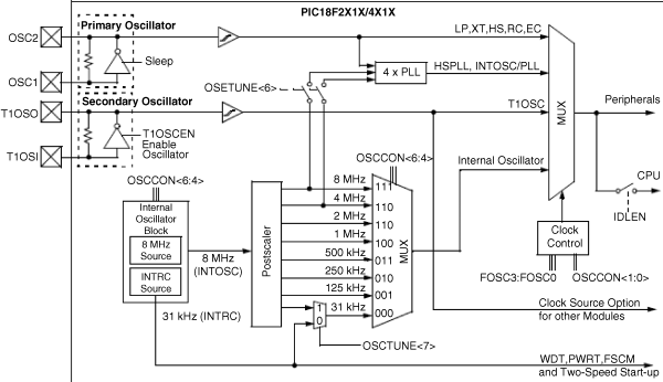
Figure 2.11 OSCCON register bit definitions. (Reproduced with permission from Microchip Inc)
The PIC18F2410 microcontroller includes a feature that allows the device clock source to be switched from the main oscillator to an alternative lower frequency clock source for conserving power. Essentially, there are two clock sources: Primary oscillator and Secondary oscillator. The primary oscillator includes the external crystal and resonator modes, external RC modes, and the internal oscillator. The Secondary oscillator is where Timer 1 is used as an internal oscillator.
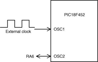
2.2.4.5 Using External Clock (EC/ECIO)
In this mode of operation, an external clock source is connected to pin OSC1 of the microcontroller. In EC mode, pin OSC2 (RA6) provides a clock output at the frequency Fosc/4. In ECIO mode, pin OSC2 (RA6) is available as a general purpose I/O. Figure 2.12 shows operation with an external clock.
Figure 2.12 Operation with an external clock
2.2.4.6 High-speed Crystal/resonator with PLL (HSPLL)
High-speed operation is possible using the Phase Locked Loop (PPL) to multiply the selected clock source by 4. The PLL operation is available either with the external crystal/resonator (HSPLL), or by using the internal clock.
In the HSPLL mode of operation, an external crystal or resonator is connected to the OSC1 and OSC2 pins, as in mode XT. The internal PLL of the microcontroller is then programmed to multiply the clock frequency by 4 to provide higher frequencies. External crystal/resonator up to 10 MHz can be used in this mode, to provide an operating frequency of 40 MHz. Bits FOSC3:FOSC0 of the Configuration register 1H are used to set the HSPLL mode (see manufacturers' data sheet for more information).
When used with the internal clock sources, the PLL can produce clock speeds of 16 MHz (with a 4 MHz internal clock) or 32 MHz (with an 8 MHz internal clock). The PLL for the internal clock sources is enabled by setting bit 6 of the SFR register OSCTUNE, as shown in Figure 2.13.
Figure 2.13 OSCTUNE register bit definitions. (Reproduced with permission from Microchip Inc)
2.2.5 The Reset
The Reset action puts the microcontroller into a known state, where the program counter is loaded with address 0 and program execution starts from this address. There are several actions that may cause a reset action:
- Power-on Reset (POR);
- MCLR Reset during normal operation;
- MCLR Reset during power-managed modes;
- Watchdog Timer (WDT) Reset;
- Programmable Brown-out Reset (BOR);
- Reset instruction;
- Stack full Reset;
- Stack underflow Reset.
In this section we are interested in the most commonly used reset actions: Power-on Reset and MCLR Reset during normal operation.
2.2.5.1 Power-on Reset
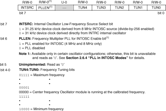
A Power-on Reset (POR) is generated when power is applied to the microcontroller and when the supply voltage rises above a certain threshold. During POR, internal parts of the microcontroller are initialised. The MCLR pin should be connected to the supply voltage with a 1 K to 10 K resistor before the POR is enabled. Figure 2.14 shows a typical POR circuit, where the MCLR pin is connected to the supply voltage via a 10 K resistor. In applications where the rise time of the supply voltage is small, it is recommended to use a diode and a capacitor in the POR circuit, as shown in Figure 2.15.
Figure 2.14 Power-on Reset circuit
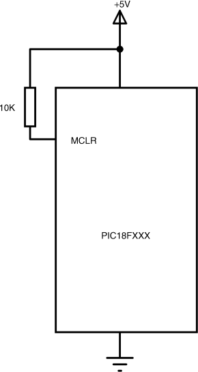
Figure 2.15 Power-on circuit for slow rising supply voltage
2.2.5.2 External Reset
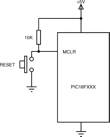
In some applications we may want to force an external reset action, for example by pressing a button. This can easily be arranged by the circuit shown in Figure 2.16. The MCLR pin is normally at logic HIGH during normal operation. Pressing the button forces MCLR to be LOW, which causes a reset action.
Figure 2.16 External Reset circuit
2.2.6 Parallel I/O Ports
The PIC18F2410 microcontroller supports 4 I/O ports named PORT A, PORT B, PORTC and PORT E. The first three ports are 8-bits wide, while PORT E has only 1 bit. The bits of a port are named as RPn, where P is the port name, and n is the bit number. For example, RB0 is bit 0 of PORT B. Similarly, RA7 is bit 7 of PORT A, and so on.
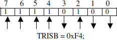
The I/O ports are bi-directional. An input port pin can easily be changed to become an output pin, and vice versa. Port pin directions must be configured before they are used. The SFR register TRIS is used to configure the port directions. Each port register has a corresponding TRIS register. Thus, for example, the TRIS register for PORT A is TRISA, the TRIS register for PORT B is TRISB, and so on. Clearing a bit in a TRIS register forces the corresponding port pin to become an output. Similarly, setting a bit in a TRIS register forces the corresponding port pin to become an input. For example, to configure pins 0, 1, 3 of PORT B to become output and the remaining pins to become input, we have to load the following values into the TRISB register:
In addition to the standard port registers, every port has a latch register. This register is called LATx, where x is the port name. For example, PORT A latch register is LATA, PORT B latch register is LATB, and so on. The latch register holds the actual value sent to a port pin. Thus, for example, when reading from a port pin, we have two choices. If we read from the latch register, then the value read is unaffected by any external device connected to the port pin. If, on the other hand, the port pin is pulled low (even though a logic HIGH was sent to the port) by an externl device, then reading the port register will give a HIGH value.
2.2.6.1 PORT A
PORT A is an 8-bits wide, parallel I/O port, with the pin configuration shown in Table 2.4. As shown, the port pins are multiplexed and can be used for different purposes. Most of the PORT A pins can be configured either as digital I/O or as analogue inputs. This port has the following registers associated with it:
- PORTA register.
- TRISA register.
- LATA register.
Register PORTA is used to write and read data from the port pins. TRISA register is used to set the port pin directions. LATA is the latch register used to read a latched output value from the port.
Table 2.4 PIC18F2410 microcontroller PORT A pin functions.
| Pin | Description |
| RA0/AN0 | |
| RA0 | Digital I/O |
| AN0 | Analogue input 0 |
| RA1/AN1 | |
| RA1 | Digital I/O |
| AN1 | Analogue input 1 |
| RA2/AN2/VREF-/CVREF | |
| RA2 | Digital I/O |
| AN2 | Analogue input 2 |
| VREF− | A/D reference voltage (low) input |
| CVREF | Comparator reference output |
| RA3/AN3/VREF+ | |
| RA3 | Digital I/O |
| AN3 | Analogue input 3 |
| VREF+ | A/D reference voltage (high) input |
| RA4/T0CKI/C1OUT | |
| RA4 | Digital I/O |
| T0CKI | Timer 0 external clock input |
| C1OUT | Comparator 1 output |
| RA5/AN4/SS/HLVDIN/C2OUT | |
| RA5 | Digital I/O |
| AN4 | Analogue input 4 |
| SS | SPI Slave Select input |
| HLVDIN | High/Low voltage detect input |
| C2OUT | Comparator 2 output |
| RA6/OSC2/CLKO | Digital I/O |
| RA6 | Digital I/O |
| OSC2 | Oscillator input |
| CLKO | Clock output |
| RA7/OSC1/CLKI | Digital I/O |
| RA7 | Digital I/O |
| OSC1 | Oscillator input |
| CLKI | Clock input |
Figure 2.17 shows the simplified internal block diagram of a generic port pin without the peripheral functions. The port pin consists of three D-type latch registers and a number of buffers. The output and input operations are described:
Figure 2.17 Generic port pin without peripheral functions. (Reproduced with permission from Microchip Inc)
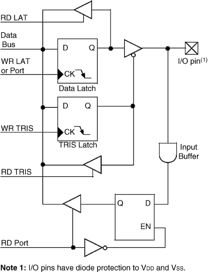
Output: TRIS register is loaded with logic 0, thus the Q output of TRIS Latch is 0, enabling the output buffer to the I/O pin. If a data is now placed on the D input of the data latch, this data appears as the output of the port pin.
Input using port input: TRIS register is loaded with logic 1, thus the Q output of TRIS Latch is 1, disabling the output buffer to the I/O pin. To read data from the I/O pin, the RD Port pin is set to logic 1, thus enabling the input latch and placing the input data on the data bus.
Input using LATx register: TRIS register is loaded with logic 1, thus Q output of TRIS Latch is 1, disabling the output buffer to the I/O pin. Setting pin RD LAT to 1 reads the data at the output of the data latch and places it on the data bus. Remember that the data read here is the actual data sent to the port output earlier, and this data is not affected by any devices connected to the I/O pin.
On POR, PORT A pins RA5 and RA3:RA0 are configured as analogue inputs. Pin RA4 is configured as digital input. SFR register ADCON1 can be used to change the port configuration. For example, setting ADCON1 to 0 × 7F configures all PORT A pins to become digital.
2.2.6.2 PORT B
PORT B is an 8-bit parallel port with the pin configuration shown in Table 2.5. As with PORT A, all the PORT B pins are multiplexed with other functions, such as analogue inputs and interrupt inputs.
Table 2.5 PIC18F2410 microcontroller PORT B pin functions.
| Pin | Description |
| RB0/INT0/FLT0/AN12 | |
| RB0 | Digital I/O |
| INT0 | External interrupt 0 |
| FLT0 | PWM fault input for CCP1 |
| AN12 | Analogue input 12 |
| RB1/INT1/AN10 | |
| RB1 | Digital I/O |
| INT1 | External interrupt 1 |
| AN10 | Analogue input 10 |
| RB2/INT2/AN8 | |
| RB2 | Digital I/O |
| INT2 | External interrupt 2 |
| AN8 | Analogue input 8 |
| RB3/AN9/CCP2 | |
| RB3 | Digital I/O |
| AN9 | Analogue input 9 |
| CCP2 | Capture 2 input, Compare 2 and PWM2 output |
| RB4/KBIO/AN11 | |
| RB4 | Digital I/O |
| KBIO1 | Interrupt on change input |
| AN11 | Analogue input 11 |
| RB5/KBI1/PGM | |
| RB5 | Digital I/O, Interrupt on change pin |
| KBI1 | Interrupt on change input |
| PGM | Low voltage ICSP programming pin |
| RB6/KBI2/PGC | |
| RB6 | Digital I/O, Interrupt on change pin |
| KBI2 | Interrupt on change input |
| PGC | In-circuit debugger and ICSP programming pin |
| RB7/KBI3/PGD | |
| RB7 | Digital I/O, Interrupt on change pin |
| KBI3 | Interrupt on change input |
| PGD | In-circuit debugger and ICSP programming pin |
As in PORT A, PORT B has the following registers associated with it:
- PORTB register.
- TRISB register.
- LATB register.
On POR, PORT B pins RB4:RB0 are configured as analogue inputs and RB7:RB5 pins are configured as digital inputs. Configuration register PBADEN or SFR register ADCON1 can be programmed to change the PORT B pin configuration. For example, when PBADEN is set to 1, all pins with analogue functions are set to analogue input mode.
2.2.6.3 PORT C
PORT C is also an 8-bit bi-directional port with multiplexed pins. The pin configuration of PORT C is shown in Table 2.6. Most points of PORT C are multiplexed with timer, USART and SPI bus functions.
Table 2.6 PIC18F2410 microcontroller PORT C pin functions.
| Pin | Description |
| RC0/T1OSO/T13CKI | |
| RC0 | Digital I/O |
| T1OSO | Timer 1 oscillator output |
| T13CKI | Timer 1/Timer 3 external clock input |
| RC1/T1OSI/CCP2 | |
| RC1 | Digital I/O |
| T1OSI | Timer 1 oscillator input |
| CCP2 | Capture/compare/PWM 2 output |
| RC2/CCP1 | |
| RC2 | Digital I/O |
| CCP1 | Capture/compare/PWM 1 output |
| RC3/SCK/SCL | |
| RC3 | Digital I/O |
| SCK | Clock for SPI mode |
| SCL | Clock for I2C mode |
| RC4/SDI/SDA | |
| RB4 | Digital I/O |
| SDI | SPI data in |
| SDA | I2C data I/O |
| RC5/SDO | |
| RC5 | Digital I/O |
| SDO | SPI data out |
| RC6/TX/CK | |
| RC6 | Digital I/O |
| TX | USART transmit |
| CK | USART synchronous clock |
| RC7/RX/DT | |
| RC7 | Digital I/O |
| RX | USART receive |
| DT | USART synchronous data |
As in the other ports, PORT C has the following registers associated with it:
- PORT C register.
- TRISC register.
- LATC register.
On power-on, all pins of PORT C are configured as digital inputs.
2.2.6.4 PORT E
On the PIC18F2410 microcontroller, PORT E is a single bit input only port, multiplexed with the MCLR (reset pin) and VPP (programming voltage pin) functions, and is available when MCLRE = 0.
2.2.7 Timer Modules
PIC18F2410 microcontroller includes 4 timer modules, TIMER 0, TIMER 1, TIMER 2 and TIMER 3. The structure and the operation of each timer are briefly described in this section.
2.2.7.1 TIMER 0
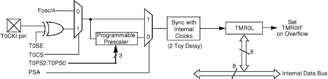
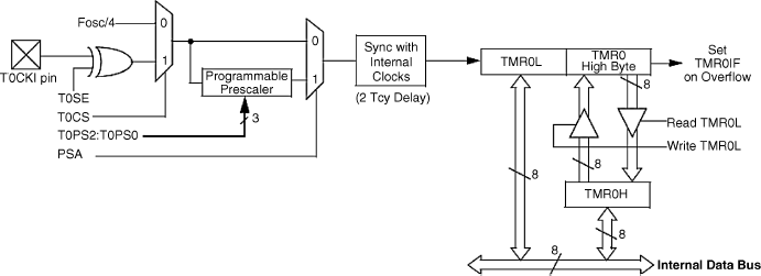
TIMER 0 operates in both 8- and 16-bit modes. The timer can be clocked from external or internal clock sources. An 8-bit programmable prescaler is provided to divide the clock frequency. An interrupt on overflow event can be declared so that an interrupt is generated whenever the timer overflows.
2.2.7.1.1 8-bit Mode
Figure 2.18 shows TIMER 0 block diagram when operating in 8-bit mode. The external clock input is the T0CKI pin. The internal clock is derived by dividing the oscillator frequency by 4.
Figure 2.18 TIMER 0 block diagram in 8-bit operation. (Reproduced with permission from Microchip Inc)
Operation of TIMER 0 is controlled by SFR register T0CON. Figure 2.19 shows the bit definitions of T0CON.
Figure 2.19 T0CON bit definitions. (Reproduced with permission from Microchip Inc)
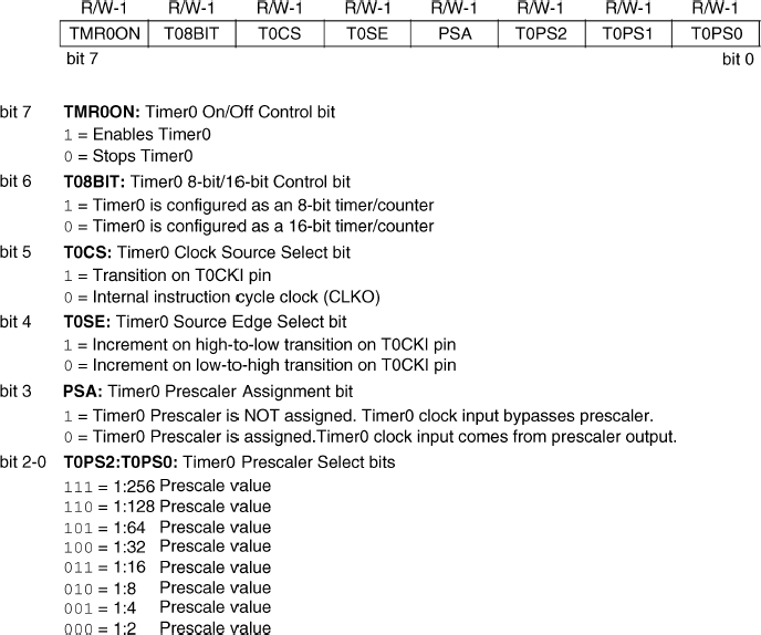
The prescaler value can be selected between 2 and 256, using bits T0PS2:T0PS0 of T0CON. TMR0L is the timer register when operating in 8-bit mode. The register counts up at every clock pulse and overflows when the count changes from 255 to 0. A timer interrupt is generated after an overflow, if the timer interrupt is enabled.
The time to overflow is calculated using the following equation:
(2.2) ![]()
where
For example, if we assume an 8 MHz clock, and the prescaler is chosen as 16 by setting bits PS2:PS0 to 011, and also assume that the timer register is loaded with decimal 100, the time to overflow will be given by:
![]()
Thus, the timer will overflow after 1.248 ms.
In most applications we want to know what value to load into TMR0L for a required time to overflow. Re-arranging the above equation, we get
(2.3) ![]()
An example is given below.
Example 2.1
It is required to generate a timer overflow after 500 μs using TIMER 0. Assuming that the clock frequency is 8 MHz, and the prescaler value is 16, calculate the value to be loaded into timer registers.
Solution 2.1
Using the above formula we get
(2.4) ![]()
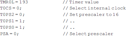
The closest integer is 193. Thus, the timer registers will be loaded as follows:
2.2.7.1.2 16-bit Mode
Figure 2.20 shows the TIMER 0 block diagram when operating in 16-bit mode. In this mode there are two timer registers, TMR0H and TMR0L. The timer high byte is not directly accessible and is updated with the help of register TMR0H. All 16 bits of the timer is updated at once. To read the 16-bit timer value, we first read the low byte TMR0L, and during this operation the high byte is loaded into register TMR0H, which can be read in a second read operation. Similarly, to write a 16-bit value to the timer register, we first write the high byte into TMR0H. Then, when the low byte is written to TMR0L, both TMR0L and TMR0H are written to the timer.
Figure 2.20 TIMER 0 block diagram in 16-bit operation. (Reproduced with permission from Microchip Inc)
2.2.7.2 TIMER 1
TIMER 1 is a 16-bit timer that can be operated as either a timer or a counter. SFR register T1CON controls TIMER 1, as shown in Figure 2.21. When operated as a timer, TMR1CS bit of T1CON is low, thus selecting the internal oscillator (Fosc/4). When TMR1CS is high, external clock from pin T1OSO is selected as the clock source.
Figure 2.21 T1CON bit definitions. (Reproduced with permission from Microchip Inc)
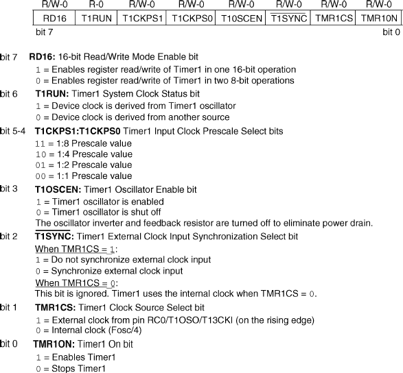
When bit T1OSCEN is high, an internal oscillator is enabled. This oscillator is intended for 32 kHz real-time clock operation, although it can operate up to 200 kHz by connecting a crystal between pins TIOSI and TIOSO. A prescaler is available, as in TIMER 0, but with only 1, 2, 4 and 8 values.
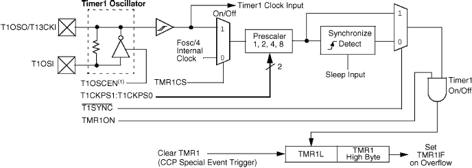
Bit RD16 controls whether the timer is loaded in one 16-bit operation, or in two 8-bit operations. When RD16 is high, the timer is loaded, as in TIMER 0 16-bit mode. When RD16 is low, the timer is loaded as two 8-bit operations. Figure 2.22 shows the block diagram of TIMER 1.
Figure 2.22 Block diagram of TIMER 1. (Reproduced with permission from Microchip Inc)
2.2.7.3 TIMER 2
TIMER 2 is an 8-bit timer, controlled with SFR register T2CON. This timer has a 1: 16 prescaler, and also a 1: 16 postscaler. Figure 2.23 shows the bit definitions of T2CON.
Figure 2.23 T2CON bit definitions. (Reproduced with permission from Microchip Inc)
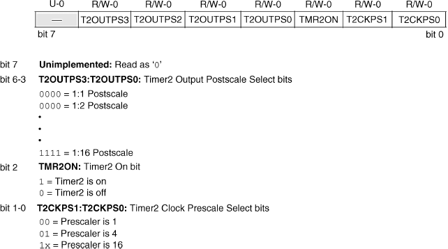
An SFR register called PR2 is loaded with an 8-bit data, which is compared to timer register TMR2. If the two registers are equal, then an interrupt is generated. This way, the timer can be used to generate pulses at fixed time intervals. TIMER 2 is generally used for the PWM and CCP operations. Figure 2.24 shows the block diagram of TIMER 2.
Figure 2.24 Block diagram of TIMER 2. (Reproduced with permission from Microchip Inc)
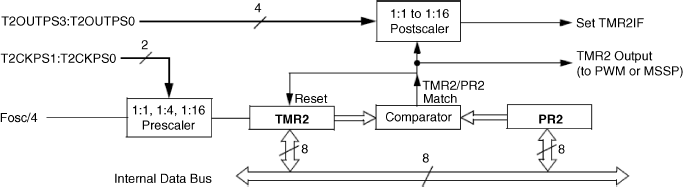
2.2.7.4 TIMER 3
The operation of TIMER 3 is similar to TIMER 1, except that TIMER 3 can operate as a 16-bit timer, as a synchronous counter, and also as an asynchronous counter. The timer is controlled with SFR register T3CON, whose bit definition is shown in Figure 2.25.
Figure 2.25 T3CON bit definitions. (Reproduced with permission from Microchip Inc)
2.2.8 Analogue-to-Digital Converter Module
The analogue to digital converter (A/D converter) module converts external analogue signals into digital form, so that they can be processed by the microcontroller. In general, an A/D converter can either be unipolar or bipolar. Unipolar A/D converters accept only positive input signals, while bipolar A/D converters can accept both negative and positive input signals. Bipolar A/D converters are frequenctly used in real-time DSP applications.
The PIC18F2410 microcontroller contains 10 unipolar A/D converter channels, each having 10-bit resolution, that is 0 to 1023 steps. These A/D converters are usually operated from a +5 V reference voltage, giving a step size of
(2.5) ![]()
Thus, the minimum voltage change that can be detected using such an A/D converter is 4.89 mV.
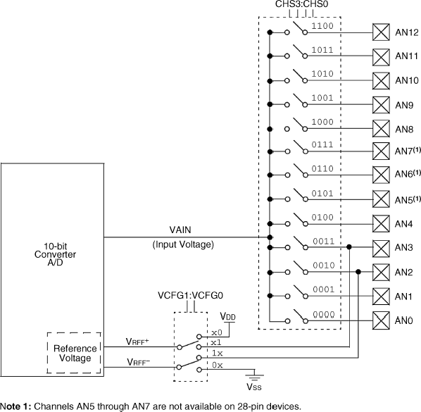
Figure 2.26 shows the block diagram of the PIC18F2410 A/D converter module. Although there are ten channels, there is only one actual A/D converter and the analogue inputs are multiplexed, only one channel being active at any given time.
Figure 2.26 Block diagram of the PIC18F2410 A/D converter. (Reproduced with permission from Microchip Inc)
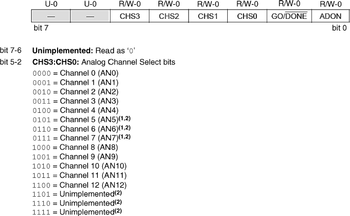
SFR register ADCON0 is used to select a channel and start the actual conversion process. Figure 2.27 shows the bit definitions of register ADCON0. Bits CHS3: CHS0 select the analogue channel to be converted into digital. Bit ADON should be set to 1 to turn on the A/D converter module. Bit GO/DONE is set to 1 to start the conversion. During the conversion process, this bit is cleared automatically and is set to 1 at the end of the conversion.
Figure 2.27 ADCON0 bit definitions. (Reproduced with permission from Microchip Inc)
SFR register ADCON1 is used to configure the I/O ports, either as digital or as analogue. The bit definitions of ADCON1 are shown in Figure 2.28.
Figure 2.28 ADCON1 bit definitions. (Reproduced with permission from Microchip Inc)
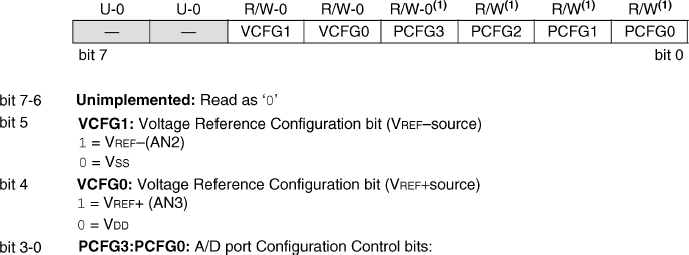
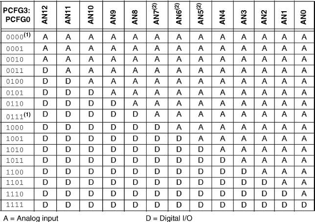
Bits VCFG1 and VCFG0 are used to select the negative and positive reference voltages. In most applications, VCFG1 is set to VSS (i.e. ground) and VCFG0 is set to VDD (i.e. +5 V reference voltage). Bits PCFG3:PCFG0 configure the analogue I/O ports. For example, clearing all these bits configure all the ten channels as analogue inputs. Figure 2.29 shows the PCFG3:PCFG0 bit definitions.
Figure 2.29 PCFG3:PCFG0 bit definitions
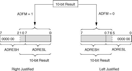
The A/D converter module has another SFR register called ADCON2, which is used to select the A/D result format and the A/D clock frequency. The bit definitions of ADCON2 are shown in Figure 2.30. The high and low bytes of the converted data are stored in registers ADRESH and ADRESL, respectively. Bit ADFM is an important bit. When set to 1, the A/D converter result is right justified, and when cleared, the result is left justified, as shown in Figure 2.31. In most applications, the result is right justified with zeroes filled in the upper 6 bits.
Figure 2.30 ADCON2 bit definitions. (Reproduced with permission from Microchip Inc)
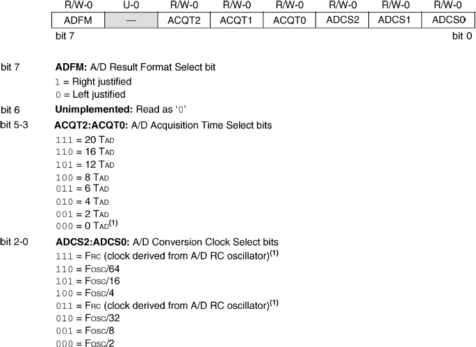
Figure 2.31 A/D converter result formatting
The A/D converter can be operated in two modes: polling, and interrupt driven. In polling mode, a conversion is started, and the end-of-conversion status is checked continually until the conversion is complete. In interrupt mode, an interrupt is generated as soon as the conversion is complete. The interrupt driven mode offers a much higher response time, but is generally more difficult to configure.
The steps in carrying out an A/D conversion are as follows:
- Set TRIS of the corresponding channel to 1 to configure the channel for input.
- Configure ADCON1 accordingly, to configure the required I/O ports as analogue.
- Configure ADCON2 bits to select the result format and the conversion clock.
- Configure ADCON0 to turn on the A/D converter module and select the required channel.
- Configure A/D converter end-of-conversion interrupt (if required).
- Set the GO/DONE bit of ADCON0 to start conversion.
- Wait until GO/DONE bit is set, or until an interrupt is generated (if enabled).
- Read the converted data into ADRESH and ADRESL.
- Repeat steps, as required for a new conversion.
It is important to take extra care when converting very fast varying analogue signals into digital. A sample-and-hold amplifier may be needed to hold the signal from changing before the conversion is started.
2.2.9 Special Features of the CPU
The PIC18F2410 microcontroller includes several features intended to maximise reliability and minimise costs by eliminating the use of external components. Some of the important features are the configuration registers and the watchdog timer.
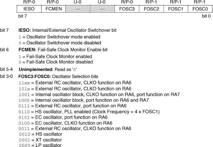
The configuration registers are usually configured during physical programming of the microconroller chip. These registers hold various important microcontroller features, such as the oscillator modes, brown-out detector configuration, watchdog configuration, and so on. In this section we look at the two most important configuration registers, CONFIG1H and CONFIG2H. Details of other configuration registers can be found in manufacturers' data sheets.
CONFIG1H is used to select the microcontroller clock mode and the clock switching logic. The bit definitions of this register are shown in Figure 2.32.
Figure 2.32 CONFIG1H bit definitions. (Reproduced with permission from Microchip Inc)
Configuration register CONFIG2H is used to configure the watchdog timer module. Figure 2.33 shows the bit definitions of this register. The watchdog is enabled by setting bit WDTEN to 1. Bits WDTPS3:WDTPS0 select the watchdog timer postscaler bits. The range can be selected from 1 to 32 768. The watchdog is clocked by the INTRC clock source. The nominal watchdog period is 4 ms. This value is multiplied by selecting a 16-bit postscaler value. Thus, the timing ranges from 4 ms to 4 × 32 768 ms, or 131.072 s (2.18 min). If the WDTEN bit is cleared, then the watchdog timer can be enabled in software by setting bit SWDTEN of SFR register WDTCON. A soft reset action is performed if the watchdog times out. The watchdog module is usually used in real-time and time-critical applications to make sure that all time-critical applications complete their tasks in the specified times.
Figure 2.33 CONFIG2H bit definitions. (Reproduced with permission from Microchip Inc)
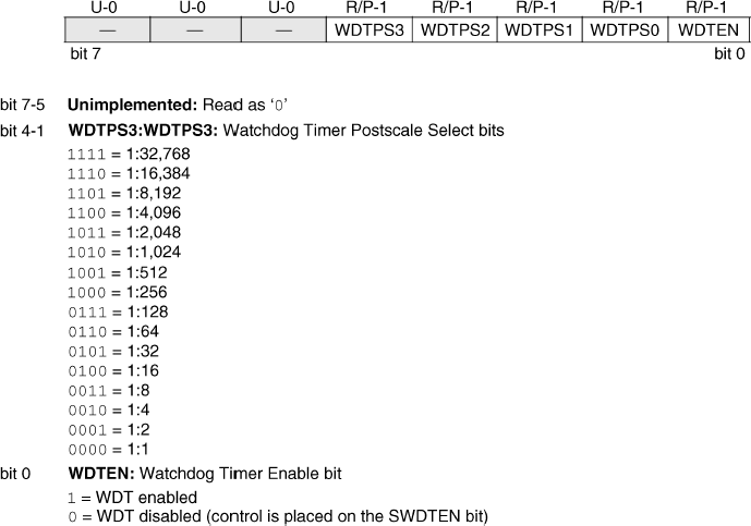
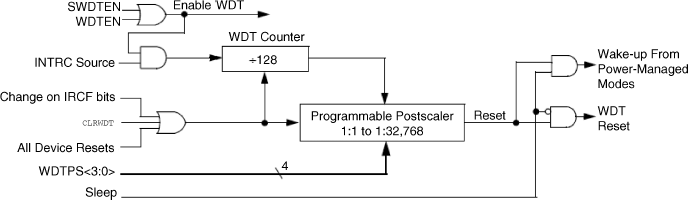
Figure 2.34 shows the block diagram of the watchdog timer module.
Figure 2.34 Block diagram of the Watchdog timer module. (Reproduced with permission from Microchip Inc)
2.2.10 Interrupts
An interrupt is an external or internal event that requires the CPU to stop its normal execution and run a program related to the interrupting event. Internal interrupts are usually generated when a timer overflows, when the A/D conversion is complete, when a character is received by the USART, and so on. External interrupts are usually generated when certain pins of the microcontroller change state.
Interrupts can be useful in many applications, such as:
The PIC18F2410 microcontroller has multiple interrupt sources, such as external interrupts via port pins RB0 (INT0), RB1 (INT1), and RB2 (INT2), PORT B interrupt when any of the pins RB4 to RB7 change state, Timer interrupts, A/D converter interrupts, USART interrupts, and so on. The interrupt sources are divided into core interrupt sources and peripheral interrupt sources. The core interrupt sources are the external interrupts and the TMR0 interrupts. Peripheral interrupt sources are the other external and internal interrupt sources. More details can be obtained from the manufacturer's data sheets. In this book we briefly look at the interrupt mechanisms.
There are 10 registers that control the interrupt operations:
- RCON.
- INTCON, INTCON2, INTCON3.
- PIR1, PIR2.
- PIE1, PIE2.
- IPR1, IPR2.
The interrupts can be divided into two categories: high-priority group and low-priority group. If a certain device requires closer attention, then it should be set as a high-priority device. If the priority is not important, then it is advisable to set all interrupts as low-priority.
The interupt priority feature is enabled by setting the IPEN bit of register RCON. If IPEN = 0, then the interrupt feature is not enabled and the processor behaves as if all interrupts are at the same priority group (this is the case with the PIC16 microcontroller family).
When the interrupt priority is enabled, two bits of register INTCON are used to enable interrupts globally. The GIEH bit enables all interrupts whose priority bits are set. Setting GIEL enables all interrupts whose priority bits are cleared. High-priority interrupts vector to address 0 × 0018, while the low-priority interrupts vector to address 0 × 0008. Interrupt sources have three bits to control their operation:
- A flag bit to indicate whether an interrupt has occured. This bit has a name ending in . . . IF, e.g. TMR0IF;
- Enable bit to enable or disable an interrupt source. This bit has a name ending in . . . IE, e.g. TMR0IE;
- A priority bit to select the interrupt priority. This bit has a name ending in . . . IP, e.g. TMR0IP.
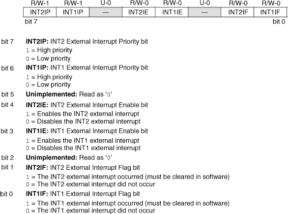
Figure 2.35 shows the bit definitions of register INTCON, which is the main interrupt control register. The core interrupt sources are controlled by registers INTCON, INTCON2 and INTCON3. The bit definitions of INTCON2 and INTCON3 registers are given in Figure 2.36 and Figure 2.37 respectively.
Figure 2.35 INTCON bit definitions. (Reproduced with permission from Microchip Inc)
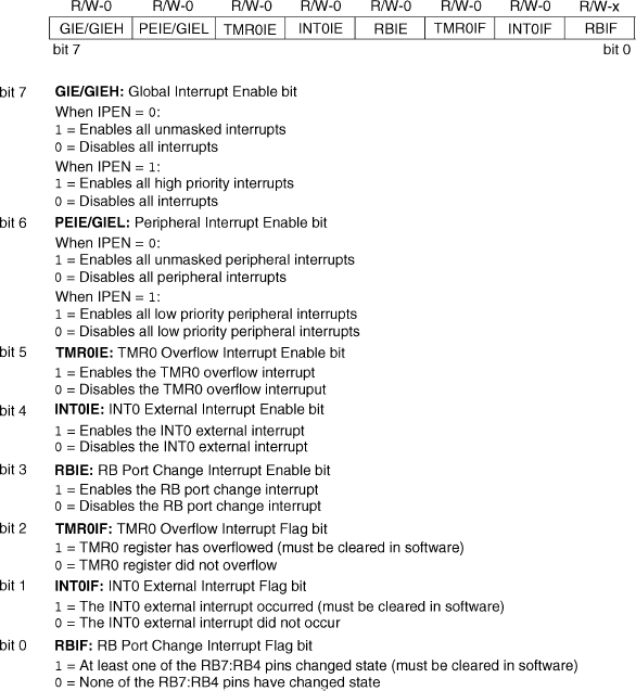
Figure 2.36 INTCON2 bit definitions. (Reproduced with permission from Microchip Inc)
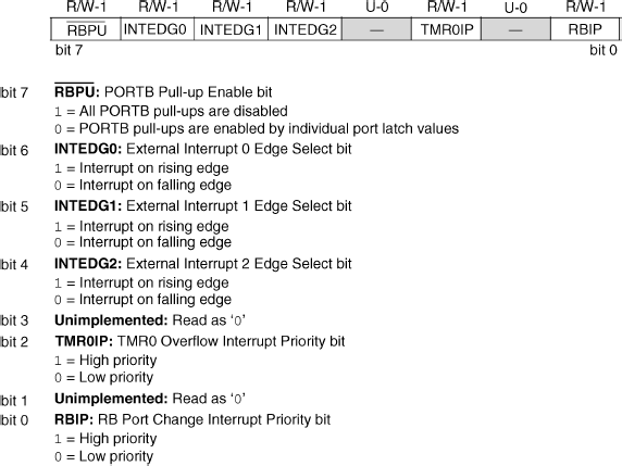
Figure 2.37 INTCON3 bit definitions. (Reproduced with permission from Microchip Inc)
2.2.10.1 Interrupts with Priority Disabled
When the interrupt priority feature is disabled, the following conditions must be satisfied for an interrupt to be accepted by the processor:
- Disable priority feature, IPEN = 0.
- Set the GIE bit of INTCON.
- Clear the interrupt flag of the interrupt source.
- Enable the interrupt bit of the interrupting device. If the interrupt is from a core device, for example the TMR0, then TMR0IE bit of INTCON must be set to 1. If the interrupt is from a peripheral device, for example the A/D converter, then enable the PEIE bit of INTCON as well as the device interrupt enable bit ADIE of the appropriate PIE register.
2.2.10.2 Interrupts with Priority Enabled
- Enable priority feature, IPEN = 1.
- Set bits GIEH and GIEL of INTCON.
- Clear the interrupt flag of the interrupt source.
- Set the priority level using the corresponding IPR register.
- Set the interrupt enable bit, using either INTCON, INTCON2, INTCON3 or PIEI registers.
As an example, the steps required to set TMR0 as a high-priority interrupt are:
- Enable the priority feature. Set IPEN = 1.
- Enable TMR0 interrupts. Set TMR0IE = 1.
- Enable TMR0 high priority. Set TMR0IP = 1.
- Clear TMR0 interrupt flag. Set TMR0IF = 0.
- Enable global interrupts. Set GIEH = 1.
2.2.11 Pulse Width Modulator Module
The pulse width modulator module (PWM) generates a PWM output waveform with 10-bit resolution from certain pins of PIC microcontrollers. Some microcontrollers have only one PWM module, while some others can have three or more. The PWM pin is identified by the letters CCPx, where x is the number of the module (e.g. CCP1).
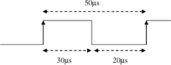
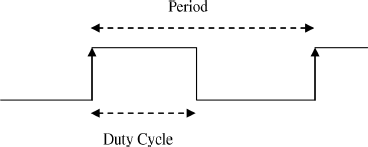
A PWM is basically a square wave signal with a specified period and duty cycle (see Figure 2.38).
Figure 2.38 Typical PWM waveform
On the PIC18F2410 microcontroller there is only one PWM module, with its pin CCP1 shared with I/O port pin RC2. On this microcontroller, the PWM module timing is controlled by Timer 2.
A PWM waveform has two parameters: the period and the duty cycle. Both of these parameters must be programmed before the required waveform can be generated.
The PWM period is given by
(2.6) ![]()
or
(2.7) ![]()
where
The duty cycle consists of 10 bits. The 8 most significant bits are loaded into the CCPR1L register and the 2 least significant bits are loaded into bits 4 and 5 of the CCP1CON register. The duty cycle (in seconds) is given by
(2.8) ![]()
or
(2.9) ![]()
The steps to configure the PWM are then:
- Specify the required period and duty cycle.
- Choose a value for Timer 2 prescaler (TMR2PS).
- Calculate the value to be written into PR2 register using the formula given.
- Calculate the value to be loaded into CCPR1L and CCP1CON registers using the formula given.
- Clear bit 2 of TRISC to make CCP1 pin an output pin.
- Configure the CCP1 module for PWM operation using register CCP1CON.
Bits 0–3 of CCP1CON register must be set to ‘1100’ to enable the PWM module. Bits 4 and 5 of this register must be loaded with the two LSB bits of the duty cycle value.
An example is given below to show how the PWM module can be set up. In this example it is assumed that we are using a PIC18F2410 type microcontroller operated with a 4 MHz clock. We further assume that the required PWM period is 60 μs and the required duty cycle (ON time) is 30 μs. The steps required to configure the various registers for this operation are:
- Using a 4 MHz clock, TOSC = 1/4 = 0.25 × 10⁻⁶ μs.
- Assuming a Timer 2 prescaler factor of 4, we have:
(2.10) ![]()
or
(2.11) ![]()
Also
(2.12) ![]()
or
(2.13) ![]()
The equivalent of number 30 in 10-bit binary is ‘0000011110’ or ‘00000111 10’
- Therefore, the value to be loaded into bits 4 and 5 of CCP1CON is ‘10’. Bits 2 and 3 of CCP1CON must be set to high for PWM operation. Therefore, CCP1CON must be set to bit pattern (‘X’ is ‘don't care’):
- The value to be loaded into CCPR1L is ‘00000111’, that is hexadecimal number 0 × 07. The required steps are summarised below:
- Load Timer 2 with prescaler of 4, that is load T2CON with
- Load 0 × 0E into PR2;
- Load 0 × 07 into CCPR1L;
- Load 0 into TRISC (make CCP1 pin output);
- Load 0 × C0 into CCP1CON.
One period of the generated PWM waveform is shown in Figure 2.39.
Figure 2.39 Generated PWM waveform