10.5 PROJECT 10.5 – External Interrupt Based Event Counter Using 4-Digit 7-Segment LED Display with Serial Driver
10.5.1 Project Description
In this project, a display module known as the BM08M04N-R is used. This is a 4-digit 7-segment LED display manufactured by Nexus Machines Ltd. This is a family of 7-segment displays ranging in size from 8 to 38 mm and available in colours of red, green and yellow. The project counts events occurring on external interrupt pin RB0/INT0. An event is said to occur when the state of RB0/INT pin goes from logic 0 to logic 1. This project is similar to Project 10.4, but here the event is interrupt driven and also the display is a 4-digit 7-segment LED module with serial driver.
The BM08M04N-R display (see Figure 10.19) has an on-board controller chip that accepts data in serial format. The display has 9 pins, as shown in Table 10.1. 36 bits of serial data are sent to the display where a logic 1 turns a segment ON. The display has two pins (pin 1 and 2) where external LEDs can be connected via on-board current limiting resistors. The cathode of the external LEDs should be connected to these pins, and the anodes to the Vledpin (pin 9). The chip enable pin (pin 3) should be LOW for the display to be enabled. The brightness pin (pin 7) provides the segment brightness. A resistor is provided on the board that can be used, or an external resistor can be used to provide the required brightness. Serial clock pin (pin 5) clocks data into the display on the rising edge of the clock waveform. Thirty-six clocks are required to clock all the data in.
Figure 10.19 BM08M04N-R display
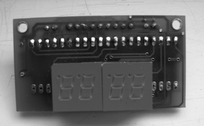
Table 10.1 BM08M04N-R pin configuration.
| Pin no | Function |
| 1 | LED 1 drive |
| 2 | LED 2 drive |
| 3 | Chip enable |
| 4 | Data |
| 5 | Clock |
| 6 | Vdd (+5V) |
| 7 | Brightness |
| 8 | GND (0V) |
| 9 | Vled |
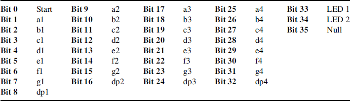
Table 10.2 shows how data should be sent to the display. The steps are summarised as follows:
- send Start bit (logic 1);
- send digits a1 to g1 of DIGIT 1 (rightmost digit);
- send decimal point (dp1) of DIGIT 1;
- send a2 to g2 of DIGIT 2;
- send dp2 of DIGIT 2;
- send a3 to g3 of DIGIT 3;
- send dp3 of DIGIT 3;
- send a4 to g4 of DIGIT 4 (leftmost digit);
- send dp4 of DIGIT 4;
- send LED1 bit;
- send LED2 bit;
- send a NULL bit.
Table 10.2 Display data.
The relationship between a number to be displayed and the bit pattern is given in Table 10.3. For example, to display number 5, we have to send 0 × B6 to the display. That is, the bit pattern ‘10110110’. The segment of each digit must be sent by shifting the bits to the left, that is the MSB bit is sent out first. Sending all zeroes to a digit blanks the digit and this is useful when we want to suppress leading zeroes.
Table 10.3 Relationship between numbers and segment patterns.
| Number | a b c d e f g dp | Hexadecimal |
| 0 | 1 1 1 1 1 1 0 0 | 0 × FC |
| 1 | 0 1 1 0 0 0 0 0 | 0 × 60 |
| 2 | 1 1 0 1 1 0 1 0 | 0 × DA |
| 3 | 1 1 1 1 0 0 1 0 | 0 × F2 |
| 4 | 0 1 1 0 0 1 1 0 | 0 × 66 |
| 5 | 1 0 1 1 0 1 1 0 | 0 × B6 |
| 6 | 1 0 1 1 1 1 1 0 | 0 × BE |
| 7 | 1 1 1 0 0 0 0 0 | 0 × E0 |
| 8 | 1 1 1 1 1 1 1 0 | 0 × FE |
| 9 | 1 1 1 1 0 1 1 0 | 0 × F6 |
| Blank | 0 0 0 0 0 0 0 0 | 0 × 00 |
As an example, suppose that we wish to display the number 3561. The steps should be as follows:
- Send a Start bit. That is send ‘1’.
- Send bit pattern for number 1 with no decimal point. That is, send ‘01100000’.
- Send bit pattern for number 6 with no decimal point. That is, send ‘10111110’.
- Send bit pattern for number 5 with no decimal point. That is, send ‘10110110’.
- Send bit pattern for number 3 with no decimal point. That is, send ‘11110010’.
- Send zeroes for the two external LEDs. That is, send ‘00’.
- Send a NULL character. That is, send 0 × 0.
The event counting will start when the STRT button is pressed.
The advantage of using a display module, such as the BM08M04, is that all the display refreshing and control functions are done on the display board. We simply send the data to be displayed in serial format. As a result of this, the microcontroller is free to do other tasks while the data is displayed.
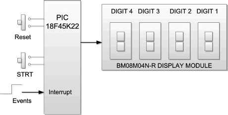
10.5.2 Block Diagram
The block diagram of the project is shown in Figure 10.20. Counting starts when the button STRT is pressed and events are recognised as external interrupts on external interrupt pin RB0/INT of the microcontroller.
Figure 10.20 Block diagram of the project
10.5.3 Circuit Diagram
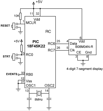
The circuit diagram of the project is simple and is shown in Figure 10.21. The STRT button is connected to pin RC0 of the microcontroller through a pull-up resistor. Normally RC0 is at logic 1 and goes to logic 0 when the button is pressed. Events are applied to the RB0/INT0 external interrupt pin of the microcontroller. The data and clock pins of the display are connected to port pins RC6 and RC7, respectively. Pin 6 of the display is connected to a +5 V power supply, and pins 3 and 8 are connected to ground.
Figure 10.21 Circuit diagram of the project
10.5.4 Project PDL
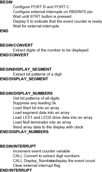
The PDL of the project is given in Figure 10.22.
Figure 10.22 PDL of the project
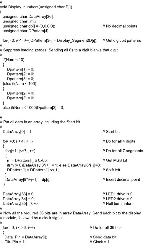
10.5.5 Project Program
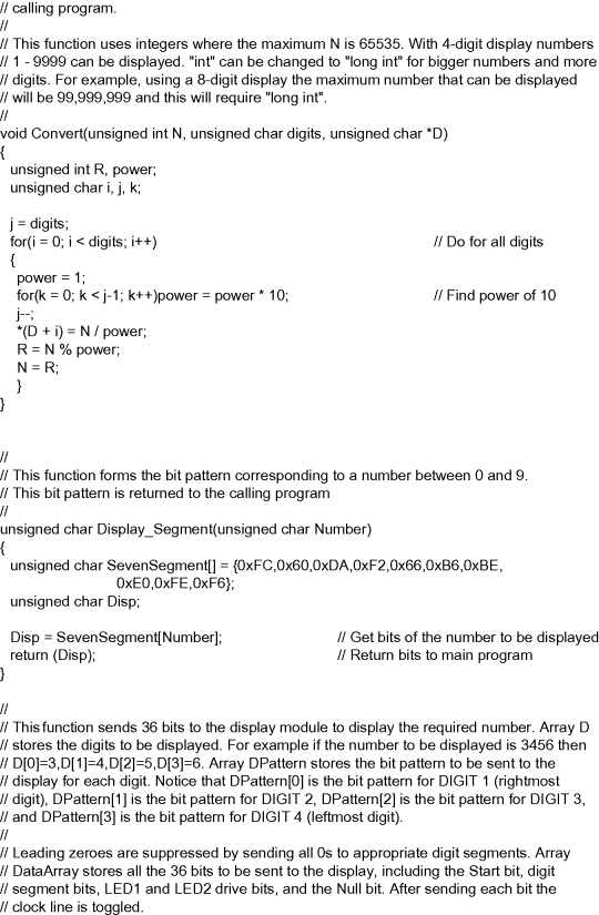
The program is named SEG6.C and the program listing of the project is given in Figure 10.23. At the beginning of the program, symbols STRT, Data_Pin and Clk_Pinare are defined as bits 0, 6 and 7 of PORT C, respectively.
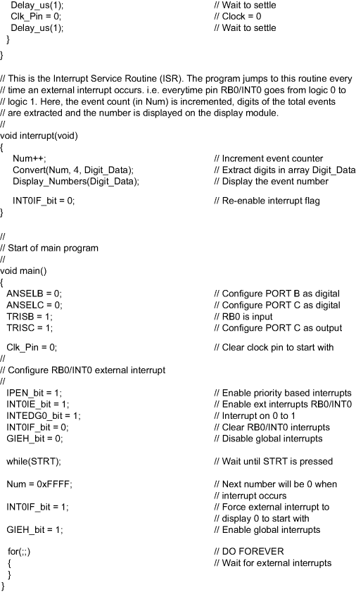
In the main program, PORT B and PORT C are configured as digital ports. Port pins RB0 and RC0 are configured as inputs, while other bits of PORT B and PORT C are configured as outputs. The program then configures external interrupts on pin RB0/INT. IPEN is set to 1, to enable priority based interrupts. INT0IE is set to 1, to enable external interrupts on pin RB0/INT. Bit INTEDG0 is set to 1, so that external interrupts are accepted on the rising edge (logic 0 to 1) of the event signal. Global interrupts are not enabled at this stage (GIEH = 0). The program then waits until button STRT is pressed. When this button is pressed, the STRT pin goes to logic 0 and the program continues. Event counter is set to 0 × FFFF, so that the next count will be 0. An external interrupt is created by setting the interrupt flag INT0IF to 1 and by enabling global interrupts (GIEH = 1). As a result of this, event count will be incremented inside the ISR so that variable Num will become 0, and the display will show 0 to indicate that it is ready to start counting events.
Function Convert extracts the digits of the current value of the event counter. This function is called with the following parameters:
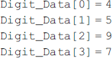
As an example, if Num = 4597, then the following values will be loaded into array Digit_Data:
Function Display_Segment forms the bit pattern to be sent to a digit of the display, in order to display a number.
The ISR is defined by using reserved word interrupt and the program jumps here whenever an external event occurs. Inside the ISR, the event counter (Num) is incremented by 1. In addition, the digits of variable Num are extracted and stored in array Digit_Data by calling function Convert. Then, function Display_Numbers is called to display the total event count number on the display. The external interrupt flag for RB0/INT pin is cleared just before exiting the ISR, so that further external interrupts can be accepted by the microcontroller.
Function Display_Numbers is the most complicated function in the program. The decimal points (dp1, dp2, dp3 and dp4) are stored in an array called dp. As the decimal points are not used in this project, they are all cleared to 0. The bit patterns corresponding to each display digit are extracted by calling function Display_Segment, and are stored in array DPattern. Notice here that the elements of DPattern are reversed. That is DPattern[0] corresponds to DIGIT 1 (the rightmost digit). The function then checks for possible leading zeroes and sends all 0s to the digits that should be blanked. For example, if the event count is say 54, that is less that 100, then digits 2 and 3 should be blanked so that the display shows ‘54’ and not ‘0054’. The next part of the function fills array DataArray with the 36-bit data to be sent to the display. Initially, the Start bit is loaded into DataArray[0]. Then the segment bits of each digit, starting from DIGIT 1, are shifted left by one and the MSB bit loaded into DataArray. This is done by logical ANDing the MSB bit with 0 × 80 to extract this bit, and then loading a 1 or a 0 into DataArray, depending on whether the MSB bit is set or not. After loading the segment bits of a digit, the decimal point of that digit is loaded, as described in Table 10.2. After loading all the necessary 36 bits, a for loop is formed to send each bit to the display, followed by a clock signal. A clock signal is defined as the 0 to 1 and then 1 to 0 transition of the display clock input. The manufacturer's data sheet specifies that the minimum clock HIGH and LOW times should be 950 ns. This is why a 1 μs delay is used after each edge of the clock signal.
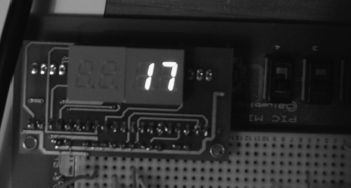
Figure 10.24 shows a number displayed on the B08M04N-R display module.
Figure 10.24 A number displayed on the display module