2.2. The ASIC Design Flow
SOC design is quite unlike board-level system design. There’s much less physical prototyping in the SOC world. Instead, SOC design verification relies almost exclusively on simulations. In fact, the SOC EDA design toolkit and ASIC design flow differ substantially from board-level design tools and flow. Figure 2.1, adapted from the Reuse Methodology Manual for System-on-a-Chip Design, presents a simplified view of the ASIC design flow called the “waterfall model” that was already showing its age when the manual was published in 1998.
Figure 2.1. This simplified representation of the ASIC design flow enumerates some of the steps required to transform a system specification into a chip layout.
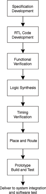
The first box of the simplified ASIC design flow in Figure 2.1 shows the creation of the system specification. For simpler ASICs, this is possibly a straightforward task. However, this simple box belies the complexity of developing system specifications for complex SOCs. We will ignore this issue, for now.
Once the system specification is complete, the simplified ASIC design flow in Figure 2.1 shows conversion of the system specification into RTL. Again, it may have been possible to compose an entire ASIC in RTL in earlier times, but SOCs aren’t so simple. At the very least, complex SOCs require the integration of numerous IP blocks including processors, memories, and other pre-coded hardware. Such IP integration may be implied by the “RTL code development” block in Figure 2.1, but it’s not obvious.
The third box in the simplified ASIC design flow is functional verification. In the simplified flow of Figure 2.1, this box represents the first time the system is simulated. Realistically, if an SOC design team waits until after the RTL coding for the entire SOC is finished, large design problems are very likely to erupt. RTL code is a hand-translated version of a system specification and converting a system specification into an hardware-description language (HDL) description is a time-consuming and error-prone manual process. If system verification only occurs after RTL coding, as proposed in Figure 2.1, errors from the overall system design will only be discovered after considerable time and effort has been expended on the coding phase. A realistic design flow for complex SOCs simply cannot postpone initial system verification until after RTL coding. To be effective and helpful, system verification must start much earlier.
After functional verification, Figure 2.1 shows logic synthesis occurring. Timing verification follows. As with functional system verification, the simple ASIC design flow of Figure 2.1 shows timing verification occurring far too late in the design flow for complex SOC design. Trying to achieve timing closure for an entire system becomes extremely difficult as system complexity and clock rates climb. Postponing all timing simulation until after logic synthesis is a prescription for disaster when designing complex SOCs.
Figure 2.1 shows placement and routing following timing verification. Once the chip is placed and routed, it can be taped out and fabricated. Figure 2.1 then shows system integration and software testing almost as an afterthought. This step is where most of the big design disasters materialize. If system integration and software testing strictly follow chip fabrication, the probability of getting a system that fails to meet system requirements are very high indeed. Many SOC design teams have faced this dismal outcome.
The Reuse Methodology Manual notes that the waterfall model worked very well for designs with a complexity of as many as 100K gates. However, the next sentence in the Manual starkly contradicts this claim: “It produced chips that worked right the first time, although often the systems that were populated with them did not.” Systems that don’t work right even if the key component chips meet spec still qualify as design disasters. Ultimately, the Manual concludes that the simple waterfall-development model simply does not work for more complex SOC designs.
Figure 2.2 shows an expanded ASIC design flow. This figure provides more detail than Figure 2.1 and shows the people involved at each design step, the tasks they perform, and the tools used to perform each of the tasks. This figure provides a better view into the steps needed to convert a system definition into a placed and routed netlist that is ready for chip fabrication. Double-ended arrows in the first column of the figure show that communication passes continually up and down the design chain so the expanded design flow has feedback paths, which the simple flow shown in Figure 2.1 lacked.
Figure 2.2. An expanded ASIC design flow details the people involved at each design step, the tasks they perform, and the tools used to perform each of the tasks.

However, Figure 2.2 still falls short of showing an SOC design flow (as opposed to an ASIC design flow) because the entire SOC design occupies just one box—a task to be performed by the system architect. System design is inherently more complex than the simple single-box representation in Figure 2.2. At the very least, the ASIC design flow shown in Figure 2.2 is dedicated to producing a chip, not a system. In particular, Figure 2.2 shows no software developers or software development. Similarly, no system-integration or system-testing tasks appear in this diagram. ASIC design flows do not adequately describe system-design tasks that must preface the work of translating RTL descriptions into silicon. Ultimately, ASIC design flows focus on producing chips, not systems. If the system isn’t right, the silicon won’t be right either.