
1.3 IMPLEMENTATION STYLES
Although implementations of electronic systems can span a number of levels of physical hierarchy, in reality implementations in semiconductor components and boards dominate. Most of designing leads to PCBs populated with standard components. Progress in component and board technology has spawned particular implementation styles. These may be classified as in Table 1–1, which shows the SSI/MSI, LSI and VLSI eras corresponding very roughly to the last three decades.
1.3.1 Era of Early Logic Families
This era ran through the 1960s and into the 1970s. It was typified by Texas Instruments and transistor–transistor logic (TTL) [TTL88], and National Semiconductor’s 4000 series, popularly called small-scale integration (SSI) and medium-scale integration (MSI). Each provided logic in the form of gates, flip-flops, register transfer components, counters, and arithmetic-logic units (ALUs), at the chip level. At the board level, these components were used in relatively small numbers on relatively small boards to provide datapath-sized, for example, 8-bit, quantities of a particular resource, such as immediate storage (registers). Typical early logic era components are shown in Figure 1–4.
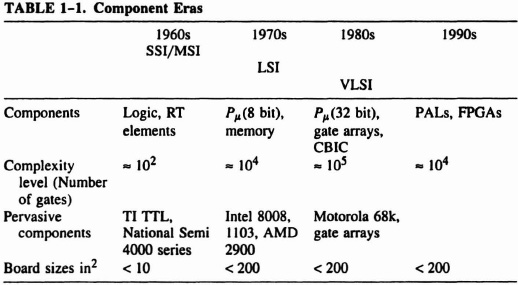
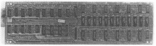
Figure 1–4. Typical early logic era components. (Photograph courtesy of P. Crockett.)
1.3.2 Era of LSI and VLSI Components
The 1970s opened with the invention of the Dynamic RAM, Intel 1103, and microprocessor, Intel 4004, and closed with the 32-bit microprocessor as a common component, for example. Motorola 68000. So technology progress spawned two major market areas, and a larger number of market segments, for example, SRAM, microcontrollers, and so forth. The logic components of the previous era continued to be used in large quantities to “glue” together the larger function chips. Boards became larger so they could accommodate a whole system on a single board, reduce cost, and eliminate the pin/wiring constraints imposed by PCB edge connectors. Figure 1–5 shows a typical subsystem of this era.
1.3.3 Era of ASICs
By the 1980s the twin drives of increasing density [Bell91] and increasing difficulty in identifying standard products redirected attention to using manufacturing technology to make ASICs. If a thousand or more gates of random logic on a chip could be wired in a cost effective way, then the “glue logic” for a system could be provided more effectively. Mask-programmable gate arrays, cell-based ICs (CBICs), and the first programmable components, programmable array logics (PALs) and field-programmable logic arrays (FPLAs), emerged during this decade as ASIC solutions. Boards remained large but delivered more function, since the “real estate” freed up from glue logic was available for primary memory or other functions. Figure 1–6 shows a typical board including microprocessor, memories, ASICs, and the first appearance of programmable components in quantity.
Taxonomy of ASICs Basically there are three varieties of ASIC: gate arrays, CBICs, and programmable logic devices (PLDs). FPGAs fall into the last of these categories. ASICs only evolved commercially in the 1980s decade as shown in Figure 1–7, which also identifies the companies that played strong parts in establishing the different product types. These companies were mostly start-ups, although there was, in the case of gate arrays, an early commercial product from Ferranti, and an internal product at IBM.
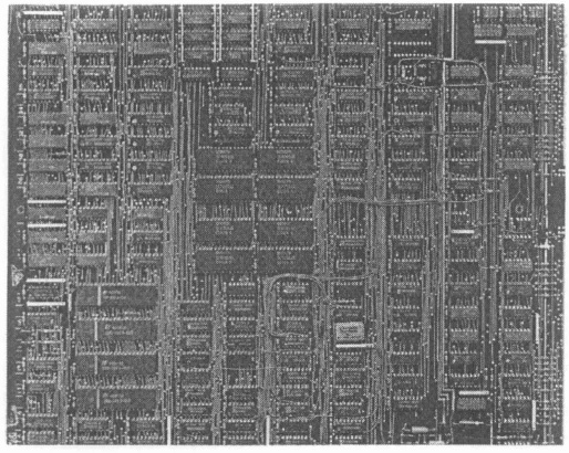
Figure 1–5. Typical large-scale integration/very-large-scale integration (LSI/VLSI) era components. (Photograph courtesy of P. Crockett.)
Each variety of ASIC is differentiated both by architectural features and by manufacturing process requirements. In consequence, a user may obtain a certain amount of custom logic in a given lead time. For example, CBICs require all the steps of an IC production process, and therefore take the longest time. Gate arrays require only the metalization steps of a production process and have a shorter lead time at a particular cost. PLDs are “manufactured” on the bench or in the application by loading bits into a control store or blowing antifuses. Figure 1–8 shows the relative times and approximate costs. Symbolic representations of the architectures are shown in Figure 1–9.
Gate Arrays Early gate arrays favored a channeled architecture in which rows, and sometimes columns, of gates were separated by wiring channels of a fixed capacity. Density levels were of the order of a few thousand gates, and this was sufficient to implement control structures and glue logic, which tend to appear random in structure. As the requirement grew to implement more regular logic structures, for example, data paths and memories, gate arrays evolved into channelless or “sea-of-gates” forms. Multilevel metalization capability and the demand for more wires, also influenced this architecture, which allows arrays of uncommitted gates to be overlayed with multiple levels of wire.
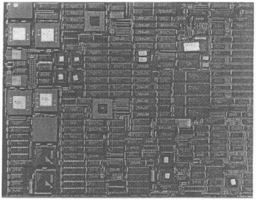
Figure 1–6. Typical ASIC era components. (Photograph courtesy of P. Crockett.)
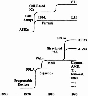
Figure 1–7. Evolution of ASICs.
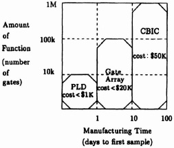
Figure 1–8. ASIC differentiators.
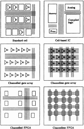
Figure 1–9. Symbolic architecture of ASICs.
Cell-based ICs Cell-based design provides the user with a library of proven cells, usually of fixed height and varying width, depending on the function performed. By the 1980s, standard cell families had evolved to provide highly complex functions, and silicon compiler technology [Gray79, Gajski88] also increased the availability of function block designs. Fabrication requires a full set of masks and processes, but these circuits provide the most dense and highest performance form of ASIC.
Programmable Logic Devices The creation of the PLD can be attributed to Monolithic Memories, which introduced the first PAL in 1978. There were early programmable products such as FPLAs [Cavlan75], but these have not been the most successful form of two-level logic product. By the late 1980s the conceptually simple PLDs were complemented by the emergence of complex PLDs in the forms of FPGAs [Xilinx92] and structured PALs [Altera87].
Growth Trends As VLSI feature sizes have been progressively reduced, the well-known rules of scaling in process technology [Mead80] have provided exponential increases in density and linear reductions in delays. The number of transistors per chip has doubled every 12 to 18 months since 1963 (Moore’s First Law). These raw transistors are used to make products such as memories, microprocessors, gate arrays, and FPGAs. The densities of these devices, measured as bits, gates, and cells per chip, have also grown exponentially (see Figure 1–10). This chart shows progress tracking Moore’s law for different products. It is interesting to note that sustainable businesses seem to emerge from getting 1000 or more useful elements, bits, gates, and cells, on a chip. For example, the commercial gate array market was pioneered by Ferranti during the 1970s with chip parts containing hundreds of gates, but it was not until a decade later that a billion dollar business developed from companies such as LSI Logic with products containing a few thousand gates per chip.
1.3.4 Era of Programmable Logic
With the emergence of complex programmable components, especially FPGAs, we can expect the typical systems PCB to resemble Figure 1–11. In this, a traditonal microprocessor is complemented by a number of SRAM-programmed FPGAs, memory parts, and possibly a special-purpose processor. The Von Neumann engine supports general-purpose computation as well as the programming of the FPGAs which, in turn, support time-multiplexed special-purpose computation.
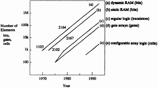
Figure 1–10. Technology progress (after Moore).
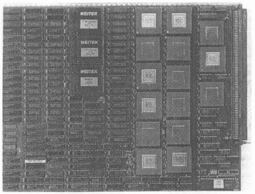
Figure 1–11. Typical components of the PLD era. (Photograph courtesy of P. Crockett.)