
4.1 THE SOFTWARE TOOLBOX
Designing is a very exciting part of engineering. Leaving aside formal definitions, it is the phase of engineering where creativity and problem solving play the most important part. These activities allow explorations of design options by trial and error, engineering judgment, “guesstimation,” analysis, measurement, simulation, breadboarding, and so forth. There is normally an overall strategy, however, to guide the transition from specification to implementation, as discussed in Chapter 1. What the engineer must do is flesh out a complete behavioral, structural, and physical description so that a design can be built and tested. With these often onerous tasks and informal procedures, we can expect tools to “get in the way” of designing. The purpose of this chapter is to be informative about the applicability of tools for FPGA design and suggest fairly loose design process flows. The treatment is based on taking a simple design example, the 7-segment display driver, through a behavioral and structural design process. This example is conceptually simple, but it is a nontrivial 4-input, 7-output function. It is also a standard transistor-transistor logic (TTL) catalog part, the TTL7446. This serves to emphasize alternatives in design process flows as well as highlighting the relevance, or irrelevance, of specific tools.
This treatment is in distinction to some more conventional approaches, mostly as found in manufacturers’ literature, which often portray the design process as a sequential walk through a small number of design steps, yielding a perfect result every time.
Another source of confusion is the plethora of tools available today. This is because the electronic CAD industry has matured over the last 10 years into a number of sustainable businesses (see Chapter 7). The design bottlenecks of the mid-1970s have been eliminated by structured design techniques embodied in new tools and often the products of start-up companies. Today such companies are mature and concentrating on marketing their products. The noise level is rising, and it is important to be able to identify the functionality of a tool to assess its relevance to FPGA design. Table 4–1 enumerates tool types against design description and level of design abstraction.
As a starting point, let us examine the primary activities in designing. These may be termed design capture, design validation, and physical design. Figure 4–1 shows possible flows between activities as well as tools that can assist in the processes within activities. Note that the starting point for designing is the existence of a specification and that the end point is the production of manufacturing data. Transitions in the flow are driven by design refinement, yielding acceptable or infeasible designs. Transitions to revise the specification are allowed.
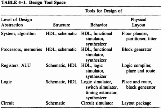
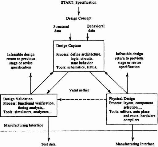
Figure 4–1. Design process flows.
Now in the case of FPGAs and our example, to get into the flow we need a specification. The specification of a 7-segment display driver is intuitively obvious, given a labeling scheme for the segments (see Figure 4–2) and no performance or electrical requirements. It could be, “drive the segments of the display to show the decimal digits 0–9 from their 4-bit binary representation as input.” Well, how do tools in a contemporary toolbox help, given this simple specification? The following sections illustrate process steps.
4.1.1 Design Capture
All design capture tools provide functions for capturing design intent. They may capture structural intent, behavioral intent, or both. They may be graphically based, for example, schematics, or language based, for example, hardware description language (HDL).
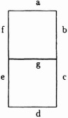
Figure 4–2. Labeling of 7-segment display.
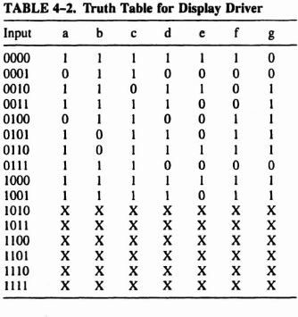
Behavioral Tools Behavioral tools address the question “what do I want this circuit to do?” Since the behavior of a circuit is a mapping between a set of input states and a set of output states, dependent on internal state (for sequential circuits), then representations, such as truth tables, logic equations, and state descriptions, are particularly useful. Truth tables are a perfectly simple and universal behavioral description. The initial truth table for the display decoder is shown in Table 4–2. With the availability of programmable array logic (PALs), several commercial behavioral HDL notations have emerged as de facto standards: ABEL, CUPL, PALASM. The PALASM2 form of the same design is shown in Figure 4–3. For the established PAL families there is even a standard file format for specifying fuse maps. In some cases these can be interpreted as truth tables, but they are really a physical description of features of a chip.
Synthesis If behavioral tools only provided methods of describing circuit functions, then they would be at least useful in refining specifications, assuming the behavioral description could be animated. To take a first step to a real manufacturable entity, however, a set of elements with defined behaviors must be hooked up to make a circuit. Now if the behavioral semantics of these elements are well understood, for example, in the case of logic gates, 2-level logic blocks like PLAs, then it is possible to transform a behavioral description into a structural composition of known parts. This is called synthesis. Trivial examples would include interpreting a logic diagram as a behavioral and structural design; mapping a set of logic equations into a PLA; decomposing an HDL into a set of register-transfer-level interconnected elements. Optimization is associated with synthesis and is applied to the automatic manipulation of logic equations to yield an optimal, in some sense, logic-level design. Today optimization and synthesis products are available from a range of companies.
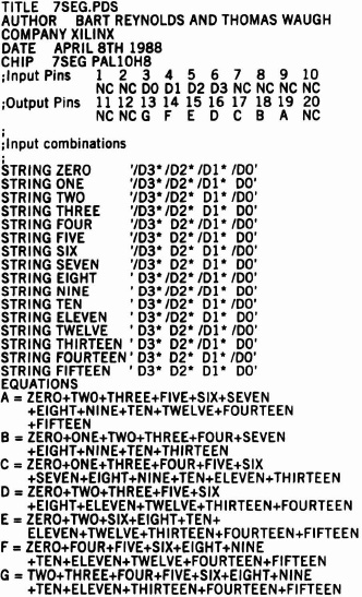
Figure 4–3. PALASM2 HDL for display driver. Figure courtesy of Xilinx Inc. ©Xilinx, Inc. 1989. All rights reserved.
Structural Tools Structural tools address capturing the design statement, “I think this interconnection of units will exhibit the required behavior.” This is the more traditional design metaphor, and it assumes the engineer is using knowledge of the behavior of units, experience, judgment, and so forth, in making a plausible design statement. Historically, this metaphor has always been supported by schematic tools. In the case of the display driver, a schematic is shown in Figure 4–4. This nonobvious design is structured across three levels of logic. The top level drawing uses a left-to-right signal flow convention.
Hardware Description Languages In recent times HDLs like VHDL [Mazor93] and Verilog have emerged as alternative textual tools for design capture. Their present existence is based on work over a long period of time to discover how to exploit the power of programming notations in hardware design. In designs with repeated structures or conditional structures, there are obvious advantages in using HDL descriptions, assuming HDL compilers exist that can sensibly instantiate the design to a low-level netlist form.
This type of HDL, compared to the purely behavioral type, can be used for structural design and/or behavioral design. The most common use is as a structural design tool to allow more rapid generation of netlist data, that is, descriptions of interconnections of gate level elements. Figure 4–5 shows a VHDL description of the schematics.
4.1.2 Tools for Design Validation
Validation tools address the question “what will this (structural) design do and how fast will it do it?” A broad spectrum of simulator products, from circuit-level simulators, which solve the underlying differential equations by numerical methods, to ad hoc functional simulators in a high-level programming language, can be used. However, with the emergence of component families at mediumscale integration (MSI), large-scale integration (LSI), and very-large-scale integration (VLSI) levels, logic level simulators have become the key design validation tools. Since FPGAs by and large deliver gate level functions, logic level simulators are particularly relevant.
Logic simulators are good at answering the “what” question, at a cost in computer time. The “how fast” question has been addressed by simulation tools in which time delays are computed more accurately, such as by using RC circuit models in switch level simulators. These have proved essential tools in getting full custom VLSI designs to operate correctly the first time they are fabricated. Now with FPGAs the computation of wire path delays can be complicated because the paths are active in the sense that routing uses transistor switches and multiplexors. It is infeasible to compute the behavior of FPGAs at switch level. Delays through FPGA cells can, however, be modeled by a finite set of constants and path-delay computations built into timing estimators. Since the performance of a circuit is usually determined by a single critical path, estimator tools can replace timing analysis.
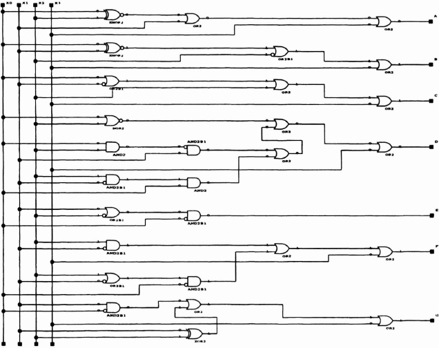
Figure 4–4. Display driver schematic.
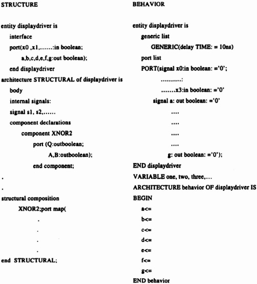
Figure 4–5. VHDL for display driver.
Our example is a purely combinational circuit, and the design can be validated by applying the ten legal input vectors and observing that the output vectors are consistent with Table 4–2.
FPGA technology raises some interesting questions on the relevance of validation tools. Simulation tools have only gained users in recent times due to rising complexity in systems design and difficulties in designing application-specific integrated circuits (ASICs). Before simulation, systems were built on breadboards with standard components and a rapid wiring technology (wrapping, Multiwire, etc). But FPGAs can be used as instantaneous breadboards and synthesis programs create valid designs algorithmically. The FPGA technology push is already creating more interest in design methodologies. One can predict that areas like design debugging will come under review now that equivalents to software debugging techniques are available in hardware.
4.1.3 Tools for Physical Design
Physical tools address the question “how do I make this (structural) design fit physical reality while meeting performance requirements?” All electronics technologies deliver finite spatial resources for building functions and communications (wires). Resources are especially tight with FPGAs, as the convenience of programmability is bought at the cost of chip area for control store.
Conceptually the simplest tool, and one that provides the essential handle on reality, is the graphical editor. For FPGAs it is most likely to be a symbolic editor since it is desirable to abstract away the underlying details of the silicon. The figures in this book mostly show symbolic artwork of two FPGA families.
The physical design process can be greatly assisted by automating the generation of random and regular logic. Block generators for regular structures such as read-only memories and programmable logic arrays are normally part of a software supplier’s package. Generators can also be custom built by engineers using ordinary programming languages. For random logic, placement-and-routing routines can be used to build both random logic blocks and to assemble blocks at higher levels.
The total spatial demand of a design includes a component for function units and a component for wires. It is important to know early on if the spatial demand of a design can be met by the spatial capacity of a particular FPGA. Estimator and fitter programs assist in this task by computing function and wire demand for a particular design for comparison with members of a standard part family.
The result of running standard physical design software on the display driver example is shown later in Figure 4–13. It shows a logic cell array (LCA) implementation and two configurable array logic (CAL) implementations: one using a ROM generator and synthesis program and the other handcrafted logic. It exposes the eternal verity that humans can outperform algorithms, in this case by a factor of 2, provided the design is tractable and there is sufficient (human) design time.
It is likely the small example we have been using is only part of a bigger design. In fact it was taken from a VLSI class exercise in which the design specification is as given in Section 4.4. In this case a key physical design activity is floor planning, in which the gross disposition of units in the design and a wiring strategy for the design are defined. Editors, generators, and place-and-route programs can all assist the floor planning phase.
Precooked designs are also a useful source of tested designs with proven layouts. These are usually found in supplier- or user-distributed libraries [Newk83].