
3.5 VLSI PRIMITIVES
In the previous sections we have considered some important current FPGA devices: many of their key architectural features are predicated on the primitives of the implementation technology.
3.5.1 Function Units
The function units of today's configurable logic devices are based on several techniques:
- RAM lookup tables: In this structure the input variables are used to select values from a RAM memory that has been preloaded with values representing the truth table of the function to be implemented. Thus all possible functions of the input variables can be implemented. Selection can use the RAM addressing mechanism in appropriately structured devices or a separate decoder taking its data inputs from RAM Q outputs. This structure offers area efficiency and predictable delays which scale well as the number of inputs is increased. It is the structure of choice for function units that attempt to implement all functions of four or more variables. An additional advantage is that it is possible with some extra overhead to allow the lookup table RAM to be used as a RAM within a user's design. The disadvantages of this implementation technique are:
(a) If the RAM addressing mechanism is used to select a lookup table output, it is difficult to organize the control store as a conventional static RAM, as is done in most of the computational logic arrays. Thus the advantages of random access to the control store for partial reconfiguration and access to internal state are lost.
(b) The large function units are inefficient at implementing common simple logic functions such as two input NANDs. This problem can be tackled by partitioning the RAM into smaller blocks and selectively combining their outputs. This can allow a single function unit to implement two functions of three variables or one function of four. Naturally, the extra multiplexing to provide this flexibility requires additional control memory and adds delay.
- Multiplexer based: This style of function unit is based on the observation that all functions of two input variables can be implemented by a single 2:1 multiplexer by placing appropriate combinations of the input variables, their inverses, and the constants 0 and 1 on its inputs. The technique can be generalized to allow more input variables and to implement latches. The main advantage of this style of function unit is that it can be implemented using the same primitives as the routing logic: in a cellular array in which function and routing are intermingled this allows for a high density layout. Multiplexer-based function units (Figure 3–13) are used in the Algotronix CAL architecture and in several antifuse programmed FPGAs. The delay through a multiplexer-based function unit is path dependent, and software can be written to optimize user designs so that the fast path through the function unit is assigned to signals on the critical path through logic blocks.
- Fixed function: The function unit provides a single fixed function. The single fixed function has the advantage of simplicity and low delay per stage. The principal disadvantage is that larger numbers of function units are required to implement logic within user designs, and the corresponding cascading of function units and routing delays results in poor overall performance.
3.5.2 Wide Gates and Long Lines
These structures are used in RAM-programmed FPGA technology to provide a low-delay alternative to the more general interconnect resources. The basic resource is a long metal wire that may potentially be connected to cell and IO block inputs and outputs. Long lines normally cross the entire array horizontally or vertically, although variations in which only half the array is crossed are also useful. Connections between long lines and cell inputs are inexpensive, since they require only an additional terminal on a multiplexer (so for the price of one bit of RAM a 4-input routing multiplexer to a function unit input could be expanded to an 8-input multiplexer to select one of four long lines as well). It is common, therefore, for a long line to have input connections to all adjacent cells and I/O blocks. Connections between cell outputs and long lines are expensive because at least one bit of RAM is required to selectively connect the cell output to the long line. Additional flexibility can be provided in the buffer between the cell output and the long line to allow, for example, wired NOR (in conjunction with a programmable pull-up resistor) or threestate (where a second data signal is used to control the buffer) protocols to be used.
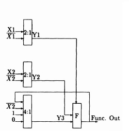
Figure 3-13. CAL function unit. Figure courtesy of Xilinx, Inc. © Xilinx, Inc. 1991. All rights reserved.
The speed advantages of long lines are dependent on switching the relatively large capacitive load of the line quickly. This arrangement requires a large buffer, which implies heavy dynamic power consumption. Static power consumption will also result in the case of wired logic. This power consumption is significant and cannot be safely neglected. When a line can be driven by several large buffers it is important to ensure that there will not be contention between those buffers: in the worst case, damage to the device can occur. This occurs when half the buffers attempt to force the common wire low and the other half attempt to force it high, so the more output connections to the wire the worse things become. The situation is complicated by threestate protocols where enable signals are generated by the user's logic, and the need to ensure that contention does not occur when the device control store contains random values prior to configuration. One way of doing this is to provide a global signal, that forces all buffers to the high impedance state. These problems with multiple-source long lines are particularly important with computational devices where the control store is reprogrammed frequently and the device must be as tolerant as possible to incorrect configurations. A computer with a halt-and-catch-fire instruction is difficult to sell!
Multiple-source long lines are relatively expensive resources in terms of device area because of the associated control store and relatively large buffers. For this reason they are usually in short supply. Even though a long line crosses the entire chip, if it is used by logic at one edge of the array, it is not available for use by a different signal at the other side. Providing programmable break points at which the long line can be segmented as required is therefore attractive architecturally. Unfortunately, the only method to achieve this segmentation in a RAM-programmed structure is to place a pass transistor switch between two metal segments of the line. When this switch is on, a buffer on one side of the switch must charge or discharge the capacitance on the other side of the switch through its series resistance. This effect rapidly removes the performance advantages of the long metal wire, although it may be tolerable for a single breakpoint.
3.5.3 Switches and Switch Boxes
The switch is the simplest routing function: it may take the form of a pass transistor controlled by a RAM cell, a fuse or antifuse, or an erasable programmable ROM (EPROM) cell, according to implementation technology. Switches allow signals to pass in both directions, although where the switch has a high impedance (such as a pass transistor) buffering circuits to restore logic levels will often force a direction on signals. A single bit of control store is required to control a switch (since it has two possible states).
Switch boxes are structures used where vertical and horizontal wiring channels cross in RAM-programmed FPGAs to mimic the rich connectivity available in mask-programmed devices. Unfortunately, RAM cells are much bigger than the contacts, vias, and gaps in metal tracks used at the switch positions in the mask-programmed technologies and so some compromises have to be made. Only a small proportion of the possible permutations can be implemented: the fact that one can connect the desired signals to terminals of the switch box is no guarantee that the required connections between them can be made. In fact, routing failures caused by limited flexibility in the switch boxes are relatively common. As an example the routing options offered by the switch boxes in the Xilinx 3000 series device are shown in Figure 3–14.
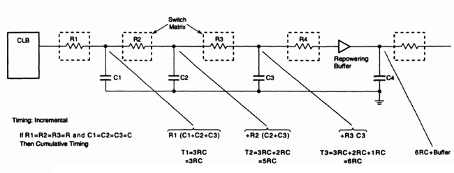
An additional factor is that pass transistors degrade the signal to such an extent that signals passing through more than a few (approximately three) must have their levels restored. Level restoring buffers are therefore commonly placed at the edge of the switch box. These buffers add delay to the signal, require control store for their own switches, and force a direction on the signal. Thus wires that pass through switch boxes and have their level restored by program controlled buffers cannot be truly bidirectional in the sense of a tristate bus with multiple sources. The accumulated resistance of switches within switch boxes also affects delay: Figure 3—15 shows this effect on the Xilinx 3000 series architecture.
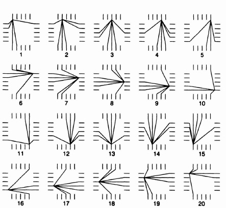
Figure 3–14. Xilinx switch box–routing possibilities. Figure courtesy of Xilinx, Inc. © Xilinx, Inc. 1991. All rights reserved.
One additional architectural option is to offer metal segments of different lengths within the wiring channels. For example, instead of every metal segment being broken at every switch box, some longer tracks that were broken at every second or third switch box could provide better delay characteristics for longer wires. One problem with this approach is the need to determine the balance between such resources a priori before manufacturing the device when user designs will make widely varying demands on the routing resources. Provision of varying length wires also complicates CAD systems that must try to make optimum choices of resource assignments.
3.5.4 Multiplexers
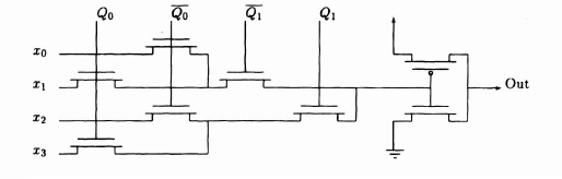
The multiplexer is a common routing structure in RAM-based technologies. The principal advantage of the multiplexer is that it allows a single bit of control store to control several switches and is hence more efficient in its use of RAM. For example, a 4:1 selector can be implemented in a multiplexer with 2 bits of RAM. A schematic for this multiplexor is given in Figure 3–16. If the same selector was built using switches, then 4 bits of RAM would be required. There are various area/performance trade-offs possible in the design of multiplexors: in particular not all paths through a multiplexer need have the same delay. For example, in a cellular structure one might notice that long wires are generally straight and optimize the paths corresponding to straight wires in the multiplexers for speed.
3.5.5 Input–Output Pad Design
The design of the input–output (I/O) pads on FPGAs must take into account many, sometimes conflicting, requirements:
- Support both TTL and CMOS voltage levels on input.
- Support bidirectional, input, output, open collector and three-statable output modes.
- Provide high drive current on output to interface with bipolar logic, drive devices such as light-emitting diodes (LED's) directly, and rapidly switch capacitive loads.
- Limit output drive to reduce power consumption, prevent overshoot, and reduce supply noise. This is particularly important in applications where high pinout FPGAs are used and large numbers of outputs may switch simultaneously.
Figure 3–15. Xilinx interconnect Figure courtesy of Xilinx. Inc, © Xilinx, Inc. 1991. All rights reserved.
Figure 3–16. Simple pass transistor multiplexer.
- Interface to crystals to provide clock oscillators, without the need for external specialized chips.
- Interface to on-chip routing resources. For many FPGA architectures, there are significantly fewer off-chip connections than on-chip routing wires at the edge of the array. The choice of which category of routing resource to connect to the pads has important consequences for the performance and flexibility of the device.
- Provide simple analog interfacing capabilities. Although no commercial FPGAs currently offer operational amplifiers, digital to analog (D/A) or analog to digital (A/D), as special-purpose resources in the pad ring, this is an obvious extension to the current technology. The programmable hysteresis characteristics and voltage level sensing features of today's devices can be used in subtle circuit configurations to build simple analog functions.
- Interface efficiently to other FPGA chips from the same manufacturer to allow arrays to be built up from multiple chips.
The provision of a flexible I/O architecture with many I/O connections can have important implications for FPGA performance and reduce the requirement for long lines within the chip. For example, one common technique is to connect a critical input signal to more than one input pad on the device (perhaps on opposite sides of the array) to reduce the length and hence the delay of internal connections between the input and the gates that use it.
The power consumption of FPGA devices is normally largely determined by the use of the I/O pins. When high pin count FPGAs are used it is vital to consider the potential power consumption (transient as well as static) of the proposed I/O configuration as well as the availability of I/O blocks. It is quite possible to melt an FPGA by ignoring this aspect of design, particularly if it is in a plastic pack.
As an example of the programmable I/Os on FPGAs Figure 3–17 shows one of the programmable I/O blocks (IOBs) on a Xilinx 3000 series device. The features offered by this IOB are somewhat richer than those offered by most FPGA IOBs.

Figure 3–17. Xilinx programmable IOB. Figure courtesy of Xilinx. Inc. © Xilinx, Inc. 1991. All rights reserved.