
6.4 SELF-TIMED FIRST-IN FIRST-OUT BUFFER
The principles of self-timed systems have been known for many years, but such systems are rarely implemented because of their complex hardware, despite the advantages of flexible data rates and the avoidance of metastability problems. The self-timed environment prototypes (STEPs) are a collection of primitives used for implementing self-timed systems. The example discussed here was proposed by Sutherland [Suther89]. Many computing applications use a first in, first out (FIFO) buffer, often implemented as a simple circular queue. This is a memory structure that will hold a sequence of data, and output it in the same order as entered. To build a circular-queue FIFO in a synchronous environment, one must use memory elements that are addressed by two counters acting as pointers. The “in” pointer indicates the address to be filled next, while the “out” pointer identifies the first location to be read. The state of the FIFO, full or empty, is calculated by subtracting “out” from “in”. FIFO control is complicated by synchronization issues and may be unreliable if the FIFO filling and FIFO emptying processes are asynchronous. Sutherland’s self-timed FIFO design is entirely different. The basic operation resembles flow through a pipeline. Data are written to one end and read out from the other. The state of each memory location is either full or empty. If a location is empty, it will pass data through. However, if it is full, it will maintain its own contents. If the first location is full, then the FIFO is full. If the last location is empty, then the FIFO is empty. The entire control circuitry consists of only one gate per location, and the resulting speed may be faster than most synchronous FIFOs.
6.4.1 STEP Elements
The self-timed environment is regulated by the handshaking of event signals. An “event” is defined here as a change of state in a control signal. A rising edge has the same significance as a falling edge and both are treated as equivalent events. An XOR gate provides an ideal merging function for events. If either input to an XOR gate undergoes an event, the XOR will cause an event on its output. A Muller-C (Figure 6–16) [Suther89] element provides a rendezvous function for events. There must be an event on each input to a Muller-C before it will cause an event to be output:
C := A.B + B.C + A.C
To understand the behavior of a Muller-C. imagine the following sequence: assume that A, B, and C are all at logic ‘0’. If there is an event on A, C stays at ‘0’, but when B rises to meet A, C also rises to a logic “1”. If B were to then have another event, C would remain at ‘1’ until A experienced an event, to match B. Only then would C fall. The Muller-C waits for events on both inputs before it outputs an event. Figure 6–17 shows the behavior of an XOR as well as a Muller-C element, as recorded by a logic analyzer.
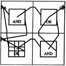
Figure 6–16. Muller C-element.

Figure 6–17. STEP waveforms.
6.4.2 CAL Implementation
Figure 6–18 shows a variant of the Muller-C element referred to as CnotM, because it has one inverted input and an active-low clear. Figure 6–19 shows the corresponding circuit. It is important to remember that in the self-timed environment, memory elements (similar to D flip-flops) must be triggered by either the rising edge or the falling edge of the control signal. Figure 6–20 shows an event-triggered D-type element, while Figure 6–21 shows its circuit. It comprises two D latches in parallel. One is latched high and the other is latched low. The output always comes from the nontransparent latch.
6.4.3 Filling the Self-timed FIFO
Figure 6–22 shows just the control structure of a 4-stage micropipeline. The output of each Muller-C can be used to control one storage location. Notice that the right-hand input of each Muller-C element is inverted, signified by a bubble.

Figure 6–18. CnotM element.
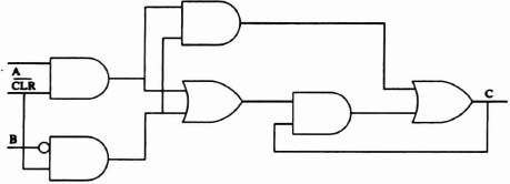
Figure 6–19. CAL CnotM circuit.

Figure 6–20. Event-triggered D-type flip-flop.

Figure 6–21. Event-triggered D-type circuit.
- Entering Data. Assume that all logic levels in Figure 6–22 are initially zero, that is, for an empty FIFO. If Rin (“request in”) is raised to a ‘1’ while R2 is a ‘0’, R1 will rise. Likewise, if R1 is a ‘1’ and R3 is a ‘0’, R2 will rise. R3 also rises, followed by R4. Now imagine that each R(n) signal is the control input to four dual-edge D-type flip-flops, that is, for a 4-bit-per-stage pipeline. Each time one of the control signals changes, the data are moved one position to the right. Eventually Rin may fall. If R2 is a ‘1’ and Rin is a ‘0’, then RI will fall. R1 and R3 cause R2 to fall, then R2 and R4 cause R3 to fall. However, Aout (“Acknowledge Output”) may not have been changed by the receiver. When R3 falls, R4 does not follow, because there has not been an acknowledge event on Aout. The FIFO now contains two distinct data values. Each stage of the FIFO receives a request signal and provides an acknowledge signal. When the next data value is passed down the FIFO, R3 is still waiting for an acknowledge from R4, so R3 will not flip. The data will only be piped as far as R2. Changing Rin a fourth time will flip R1 only.
Figure 6–22. Micropipeline control structure.
- A Full FIFO. One could now imagine that new data were placed on the input to the FIFO and Rin was toggled. No event would occur on R1. The “write request” would not be acknowledged. When Rin and R1 are not equivalent, the FIFO is full. The exception to this rule would be the short time that it takes R1 to flip under normal operating conditions but, even then, it would be destructive to toggle Rin when R1 has not even had the chance to change.
- Reading from the FIFO. Each stage reacts to the previous stage by acknowledging that it has received the data. If stage 4 does not contain the data in stage 3, then stage 4 has never acknowledged stage 3. In the same way if we have read the output of the FIFO and would like it to display the second value entered, we simply toggle Aout. Refer to Figure 6–22 again, and recall the values of the control lines:
R1 = ‘0’ R2 = ‘1’ R3 = ‘0’ R4 = ‘1’
If Aout were raised to ‘1’, R4 would be driven to a ‘O’. The change in R4 would trigger R3 to a ‘1’, and R2 would change to a ‘O’. If we toggle Aout again, the control values will shift right again, along with the data. - Empty Test. When R4 is equal to Aout, the FIFO is empty. The reading device should only read from the FIFO, when R4 (Rout) is not equal to Aout. If they are equal, then a “read request” has not occurred, and there are no data to read.
- Functional Demonstration. Figure 6–23 is a test, performed in the sequence described earlier. It may be helpful to reread the beginning of this section while reviewing the figure.

Figure 6–24 shows CAL implementations of the four-stage control unit. Figure 6–25 shows the same construction with the event-triggered flip-flops inserted.
6.4.4 Designing in CAL
The design was tested on the CHS2×4 board described earlier in this chapter. At first the design was spread over the array of CAL chips, with no regard to chip boundaries, but unreliable operation was traced to the fact that some Muller-C elements were split between chips, introducing an extra feedback loop delay of about 40 ns. The design was relaid to avoid splitting and the problem eliminated.
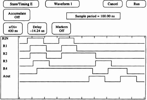
Figure 6–23. Filling the CAL FIFO.
6.4.5 A Full-custom Self-timed FIFO
While the CAL configuration is eminently suitable for experiments with self-timed systems, it carries a lot of structural overhead, that is, configuration memory and multiplexer control. To place these complications in perspective, a custom chip was designed for the self-timed environment, and was fabricated by a 2-μ bulk CMOS n-well process. One structure on this chip is a 15-stage FIFO constructed with the self-timed design principles described earlier. It has been tested with the same measuring equipment used for the CAL implementation. Data can be passed through 12 stages of the FIFO in about 210 ns. Figure 6–26 shows the waveforms of R2, R5, R8, R11, and R14 in the STEP FIFO as it passes data forward. However, this speed is not maintained through the I/O pads. On-chip, the FIFO would appear to be able to handle switching spèeds as high as 57 MHz, but with the pads included the maximum speed is 29 MHz. Data are preserved at these speeds.

Figure 6–24. CAL micropipeline.

Figure 6–25. CAL FIFO.

Figure 6–26. Full custom test.
6.4.6 Conclusions
The CAL design of a STEP FIFO runs at approximately 15 MHz, while the custom VLSI implementation runs at 29 MHz. It is surprising that the CAL configuration is not substantially slower. This indicates that in the future, most experiments could be done in CAL only, since it is nearly as fast as a custom chip.