
5.6 MULTIPLIERS
Multiplier designs are a simple way of studying different varieties of digital logic designs. It is possible to develop different multiplier examples to study the varieties of design approaches and implement these designs using FPGAs. In the following sections Xilinx 3000 implementations are assumed, but the approaches vary from fully automated to handcrafted with corresponding gains in performance.
5.6.1 Parallel Multipliers
The simplest of the multiplier designs is a parallel-combinational logic multiplier. This multiplier produces a result by adding the partial products of equal binary weight with the carries of the lower binary weight. The design consists simply of AND, OR, XOR, and inverter gates at the top-level schematic.
Schematic Entry Figure 5-31 is an example of a 4- × 4-bit combinational logic multiplier. The design was created using ViewLogic WorkView. Using CAD tools, a logic design can be entered directly as a top-level schematic, manually connecting gates together. To obtain more information about creating a schematic design, refer to the current Xilinx and/or Viewlogic WorkView manuals.
Functional Simulation It is always a good idea to check the design functionality before actually continuing with the creation of the layout file. The software used to create the schematic design provided support for a functional simulation of the schematic circuit. Refer to Figure 5–32.

Figure 5–28. Comparator. CAL block.
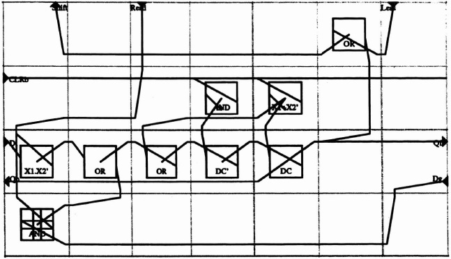
Figure 5–29. Control: CAL block.

Figure 5–30. Overall layout of sorter.

Figure 5–31. 4- × 4-bit combinational multiplier.
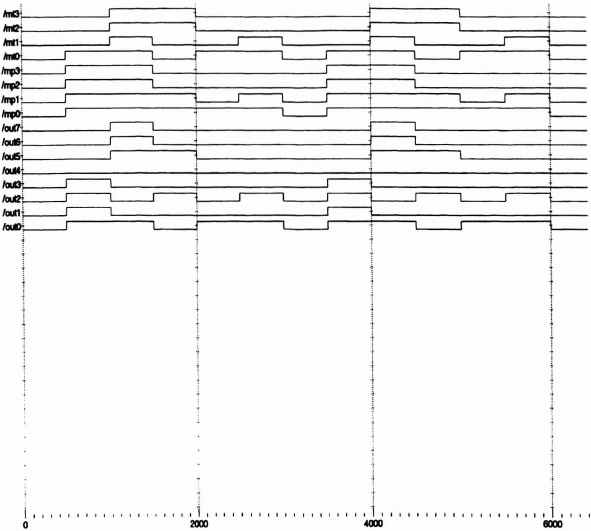
Figure 5–32. Waveform for functional simulation.
File-conversion Process In order to be able to create a Xilinx layout for the parallel multiplier, it is necessary to follow a series of steps to convert the file to the correct format. The file-conversion process consists of the following steps:
- Generate a “wirelist” (net) file from the schematic level file
- Generate a netlist file from the wirelist file
- Generate a layout file using the automatic router
Speed Most of the technology used today requires the use of high-speed circuits. The speed performance of the Xilinx design will be affected by several factors: choice of part being used, the arrangement of the programmed logic within the circuit, and the efficiency of the layout itself.
XACT Design Entry It is possible to enter a design directly by using XACT (the Xilinx design editor). This can be done by configuring the blocks directly, using logic expressions instead of entering a schematic. Figure 5–33 gives an example of the multiplier as entered using XACT.
5.6.2 Serial Multiplier with Parallel Addition
Another example of a multiplier circuit is a serial multiplier. The main difference between the parallel logic multiplier and the serial multiplier is the introduction of memory and timing in the design.
Schematic Entry Figure 5–34 is a schematic for a serial parallel multiplier created using ViewLogic WorkView.
The serial multiplier can be processed as before to generate the Xilinx layout file. Figure 5–35 shows the serial multiplier layout configuration for a 3000 family Xilinx chip.