
6.7 PLACE-AND-ROUTE ACCELERATION
The place-and-route subsystem of the Algotronix CAD software uses a simulated annealing algorithm to repeatedly generate and evaluate potential placements for a user’s design. In the later stages of this process, the computer attempts to completely route the current placement. This step of the procedure is very computation intensive and results in long run times for the software. In this section we present a hardware acceleration tool for this application, which runs on the CHS2×4 board.
6.7.1 The Global Routing Algorithm
The global routing problem for CAL is to route a set of nets successfully, each of which has a single source and one or more destinations using the multiplexer routing resources of the CAL chip. The nets contend for multiplexer resources and the algorithm will fail if more than one net requires a particular multiplexer to route. In this case, the current placement will be rejected.
Each net is routed individually using a wavefront expansion algorithm, so the order in which nets are routed is of critical importance and it is usually necessary to rip up previously routed nets and retry nets in a different order to route a design successfully. The hardware accelerator described here allows the algorithm to very rapidly determine whether implementing the current net using a particular multiplexer will cause any of the currently unrouted nets to fail to route. That is, it answers the question: Given the present allocation of multiplexers, is it possible to complete a connection between cell (x1, y1) and (x2, y2)? Figure 6–41 shows a graphical representation of the output of the algorithm when run on the control CAL routing of Figure 4–27. The square marked “S” represents the source cell of the net, “.” squares are reachable, and “U” squares cannot be wired to because of blocks caused by multiplexers assigned to other nets.
6.7.2 Hardware Architecture
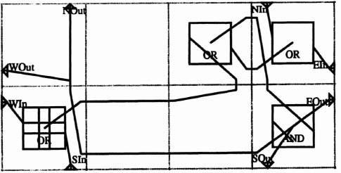
Figure 6–42 shows the basic input and output connections to a CAL cell. Each output from the cell has a dedicated multiplexer that can select any of the other inputs to the cell or the function unit output. Figure 6–43 shows a circuit that can model the routing possibilities of the cell: if any of the cell inputs go high, then all the cell outputs go high. We can build an array of these blocks in one-to-one correspondence with the array of CAL cells we are attempting to route.
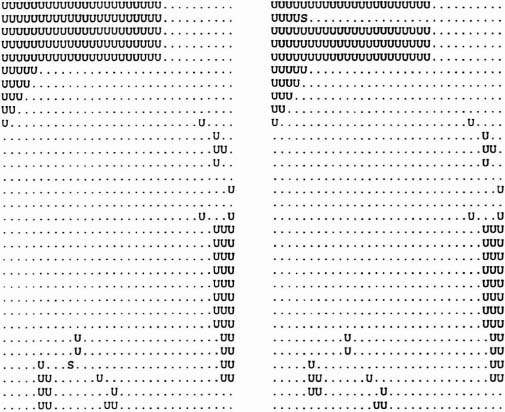
Figure 6–41. Reachability data for control CAL.
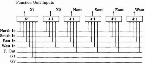
Figure 6–42. CAL cell routing. Figure courtsey of Xilinx, Inc. © Xilinx, Inc. 1991. All rights reserved.
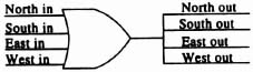
Figure 6–43. Hardware routing model of CAL cell.
If we think of logic 1 as representing “reachable” and logic 0 as representing “notreachable” and insert a single logic 1 into the array at the source point of the net of interest, then logic Is will propagate to all reachable cells.
There are two remaining considerations:
- 1. It is necessary to force all the model circuit’s outputs low before inserting the single logic 1. If there are any spurious logic Is elsewhere in the circuit before starting the test, then these will propagate at the same time as the “real” 1, potentially resulting in unreachable cells being marked as reachable. Initialization is achieved by inserting an AND gate on the output of the OR gates with its input controlled by the global signal Gl: thus when Gl is low, all outputs will be forced low.
- The model at present represents an array prior to any configuration: we need to represent multiplexers currently assigned to the user’s design. This is done by dynamically reconfiguring the logic within the blocks. We can represent a multiplexer assigned to another net by deleting the corresponding input to the OR gate in the adjacent cell. This is done by reconfiguring the function unit from OR to X1 or X2, or from X1 or X2 to constant ZERO, according to which input is to be deleted.
6.7.3 CAL Layout
The CAL layout for a single repeating block is shown in Figure 6–44. Since it is 4 cells wide and 2 cells high, we can model a single CAL chip on a 4-by-2 array of CAL chips contained on a CHS2×4 board. This layout is not optimized for density, since the goal was to model a single CAL device on the board and leaving extra space made some implementation details easier.
6.7.4 Software
The software required to implement the maze routing accelerator is in two parts:
- A simple (30 line) laura program builds the array of cell models based on the basic repeating cell design described earlier.
- Run-time software dynamically reconfigures the cells within the array to remove inputs to the OR gates where multiplexers are assigned to other nets. It also uses dynamic reconfiguration to insert a logic 1 at the trial net’s source and to read back cell outputs to determine reachability.
Figure 6–44. CAL layout for cell routing model.
6.7.5 Performance
The hardware architecture will propagate a signal across a cell in about 30 ns. This is sufficiently fast that performance is entirely limited by the program that accesses the board. This must calculate the memory addresses required, that is, to add the logic 1 at the net’s source and read back whether its destinations have been reached. It is expected that integration of the hardware accelerator within the place-and-route system would result in substantial overall performance increases.
This example shows the potential benefits of a general technique where the FPGA logic is used to directly model the situation of interest, using direct access to the control store to set up initial conditions and read back results.