
8.3 FIELD-PROGRAMMABLE INTERCONNECT
This section is concerned with a simpler concept, that of field-programmable interconnect, that is, an FPGA without its on-chip logic. This type of chip allows much more flexibility in assembling systems composed of multiple FPGA chips, possibly with other components such as random-access memory. The chips required are conceptually crossbar switches, that is, they permit any signal to enter the chip and be broadcast to any number of other signal pins. This additional flexibility in interconnection from chip-to-chip gives flexibility in partitioning designs across multiple FPGA chips, and is important in keeping down the cost of design iterations at the printed-circuit-board level. It also has practical advantages in locating errant signals at debugging time.

8.3.1 Aptix Field-programmable Interconnect
The System Verification Bottleneck Over the last several years boardlevel system complexity has dramatically increased, largely due to the fast-paced evolution of advanced integrated circuits. Such advances in silicon inevitably provide products with improved function, performance, integration, and cost. However, they have also forced the system verification process to become a significant bottleneck in the development cycle. As verification methodologies, printed-circuit-board (PCB) prototyping and simulation both have their benefits, but neither can provide the revolutionary change needed to support the increasing time-to-market emphasis of today’s electronic products. Aptix Corporation provides a solution to the system verification challenge and beyond, through a new technology called programmable interconnect.
Prototype Form and Function Conventional prototyping offers a verification vehicle with the form and function of the final PCB design. This allows a hands-on debug approach that often uncovers real-world problems too difficult or time-consuming to find through simulation. Prototyping also makes possible replicate copies for other purposes in the development process, including software integration, test, and customer evaluation. Due to these attributes, it is rare to bypass a PCB prototype before a final production version is committed to. However, advances of today’s high-density microprocessors, peripheral/support chip-sets, application-specific integrated circuits (ASICs), FPGAs, and complex programmable logic devices (CPLDs), have forced initial system verification away from prototyping and more toward simulation. Factors such as high-density surface-mount packaging, higher interconnect complexity (pins/square inch) and greater functional complexity make gathering and observing data, and making design modifications, much more difficult with a physical prototype than in a computer-aided engineering (CAE) simulation environment.
Simulation Flexibility System simulation offers the key verification benefit of flexibility allowing for easy experimentation, extensive observability, and quick changes, all in an environment fully integrated with design entry tools. But as powerful and convenient as simulation tools are, they are only as effective as the test vectors and simulation model parameters provided. Creating vectors for all possible cases can be very time-consuming, adding significant time to the verification process. Even if a thorough set of vectors is created, there will always be variations between the real world and the simulated environment, making physical prototyping inevitable. Additionally, when long simulation efforts are conducted, other development tasks, like software integration, must stay on the side lines waiting for a physical prototype.
Programmable Interconnect: The Missing Link This comparison of simulation and prototyping is not to state that one methodology is better than the other, but to point out that both have a place in system verification. Unfortunately, one is in a CAE environment and the other is in the laboratory. The ideal solution would offer the flexibility of simulation, the form and function of a physical prototype, and a link between the CAE and laboratory environments.
As the next logical step in the evolution of programmable devices, Field-programmable interconnect components (FPIC),* bring the benefits of programmability to the system level by enabling totally “programmable hardware.” FPIC devices, combined with the design tools and hardware that support them, offer a development and verification vehicle with true form, function, and flexibility. The end result is faster and more thorough verification, earlier product integration, and accelerated time to market (see Figure 8–13).
Field-programmable Interconnect Components Continuing the evolution started by programmable memory and programmable logic (see Figure 8–14), programmable interconnect holds the key to complete system programmability. History has shown that programmable technologies initially are used in a laboratory environment, enhancing development and ease of experimentation. As experience by more users is accumulated, and component prices are reduced, applications rapidly expand into final manufactured products. With similar benefits of programmable predecessors, FPICs provide the high-density interconnect architecture, performance, and packaging needed to make programmable interconnect a reality.

Figure 8–13. Programmable hardware: form, function, and flexibility.

Figure 8–14. Programmable hardware evolution.
The first two members of the FPIC family include the FPIC AX1024D (FPIC/D) and the FPIC AX1024R (FPIC/R). Each has 1024 pins arranged in a 32 × 32 pin matrix. The vast majority of these pins are passive path bidirectional I/Os (typically 120 ohms, 20 pF) that can be interconnected to any pin or group of pins through a programmable routed-array architecture. Rich in routing resources, the unique FPIC architecture achieves 100% routability for most applications. Designed in an advanced 0.8-/μ CMOS technology using over 1M transistors, FPIC devices deliver high-speed I/O interconnects as fast as 5 ns. Interconnect programming elements based in CMOS SRAM allow the architecture to be quickly reprogrammed in the system through a high-speed serial interface. The FPIC/D and FPIC/R are designed for interconnection of signal ranges from 0 V to 5 V.
Sporting equivalent routing and performance capabilities, the primary difference between the two FPIC devices has to do with their packaging and functional utility. The FPIC/D is optimized for development and is housed in a screw-mount removable 1024 gold button socket. Protruding from the socket is a 64-pin diagnostic cable providing an observability window for selectively accessing any of the pins. The diagnostic capabilities, explained in more detail later, make the FPIC/D ideal for initial prototype development and verification. The FPIC/R complements the FPIC/D by providing an interconnect solution geared toward replication and stand-alone operation. It is housed in a lower-cost surface-mount pin-grid-array (PGA) package, allowing permanent attachment. Of the 1024 pins on FPIC devices, approximately 20 are used for the programming interface and power, 64 are reserved for diagnostics (FPIC/D only), and 940 are available for user-defined programmable interconnect purposes.
Programming of FPIC devices is handled through serial interface. For the FPIC/D, this interface is typically controlled externally through a connection to a PC or workstation. For the FPIC/R the interface may optionally be configured using a stand-alone memory/interface circuit that initializes the FPIC/R upon power-up. The configuration data used for programming FPIC devices can be generated using the Aptix Development System.
Applications for the FPIC devices address a broad spectrum of interconnect needs, including system prototypes and breadboards; user-specific/configurable PCBs; application configurable processors; test interfaces; as well as programmable connector and switching matrix applications. Using FPIC devices for system prototyping, in conjunction with other programmable components (PLDs, FPGAs, microprocessors, micro controllers, digital signal processors (DSP), and programmable memory), can further enhance the design verification process, allowing faster, more flexible, and thorough product integration.
Field-programmable Circuit Boards Field-programmable circuit boards (FPCBs)† are unique PC boards designed to take full advantage of the high-density interconnect and observability of FPIC devices. FPCBs provide an ideal vehicle for system prototyping by utilizing FPIC/D devices for development and FPIC/R devices for replication. Programming FPIC devices is handled through a connector on the FPCB that interfaces to a PC or workstation via a cable and host interface module.
Unlike conventional PCBs, all FPCB component pin traces are routed to a centralized matrix of pads where an FPIC device provides for pin-to-pin interconnect (see Figure 8–15). FPCBs can have one or more FPIC device for interconnection, depending on the pin density required. A single FPIC device on an FPCB can provide up to 940 user interconnect pins. When higher pin densities are needed, multiple FPIC regions are used. Interconnections between FPIC regions are supported through assigned “global” interconnect pins that enable a direct link between FPIC devices. For example, Figure 8–16 shows an FPCB in an AT form factor with three FPIC regions of approximately 750 component pins and 200 global pins. To connect one pin of a device to another pin, the signal is routed through the local FPIC device, and if necessary, through the global pins to another FPIC region for final connection to a component pin. In this scheme signals will travel through a maximum of two FPIC devices.
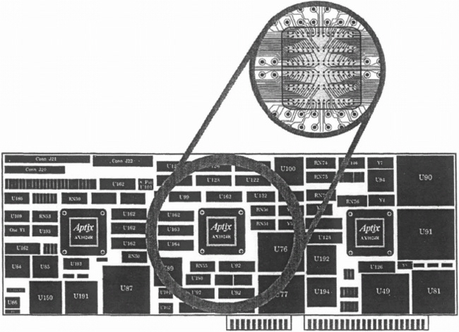
Figure 8–15. All FPCB component pins connect to a matrix of pads located under the FPIC device.

Figure 8–16. Each FP1C support regions of component pins that connect to other regions through global pins.
The through-hole pattern on an FPCB is arranged with repeated rows spaced at 100 mil, 300 mil, 100 mil, 300 mil, and so on. This industry standard pattern not only directly supports insertion of standard 300-mil DIP components, but allows adaptation of a wide variety of larger through-hole and surface mount components through the use of socket adapters. FPCBs are equipped with pin sockets in each through-hole location, allowing components to be easily inserted and removed.
Between each 300-mil row of pins are power or ground pads that provide direct access to every pin for connecting component power supplies, decoupling capacitors or pull-up/pull-down resistors. Additional user-supplied voltages (outside the 0 to +5-V supply range) can be accessed on the perimeter of the FPCB hole pattern. Pin densities of the FPCB pattern are approximately 50 pins/in2, which is currently above industry PCB averages of 32 pins/in2.
FPCBs from Aptix come in a variety of standard form factors, the first of which includes a general-purpose FPCB, along with two for standard busses, an AT-FPCB and a VME-FPCB. These initial FPCBs will satisfy a large number of general development applications; however, for those with more specific needs, the Aptix FPCB compiler software makes it possible to create user-customized FPCBs. Per user specification, the FPCB compiler creates Gerber plots for the FPCB hole pattern and its unique routing architecture. The Gerber plots can then be integrated with existing PCB layout software, allowing company-specific form factors, connectors, and special circuitry to be maintained while providing the interconnect flexibility of an FPCB with FPIC devices.
The Aptix Development System The Aptix Development System provides everything needed to effectively implement FPCB prototypes using FPIC devices (see Figure 8–17). The system lets system designers do front-end design with existing PC or workstation-based schematic capture software. When the design is ready for prototyping, a netlist is created for use by the Aptix Development System software.
Within the software there are five primary stages in creating an FPIC/FPCB design. These stages are setup, partitioning, placement, routing, and programming. In the initial setup stage several preliminary design issues are addressed, including FPCB board selection, netlist importation, package assignment (if not already assigned via the netlist), and critical net prioritization. After setup is complete, the components can be automatically and/or manually partitioned between multiple FPIC regions. Components on the FPCB can then be placed using either automatic or manual placement methods or a combination of both. Once this is accomplished the actual component interconnections from the netlist are automatically routed for programming into the FPIC. All automatic partitioning, placement, and routing operations are guided by critical net priorities, resulting in the fastest routes for the most critical nets. After the board is populated with the design components, the routed FPIC programming file can be downloaded to the FPIC device via the serial port and host interface module. Throughout the development process the Aptix software provides flexible design file management, detailed design statistics and information, and assembly documentation to ease the FPCB prototype process. Initial platforms supported by the Aptix Development System are SUN SPARCstations using X-Windows and on 386/486 PCs operating under Windows.
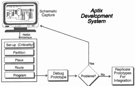
Figure 8–17. The Aptix Development System design flow.
The FPIC/FPCB Development Environment Once an FPIC programming pattern is downloaded to an FPCB, debugging takes on an entirely new form compared to conventional prototyping. For example, although all the components may physically reside on the FPCB, the software allows components to be electrically removed or isolated through selective placement and routing. This makes possible a step-by-step debug approach whereby incremental blocks of logic can be analyzed in a fast and interactive way. If actual component interconnections need to be altered or added, such changes can be made in the original schematic and then imported for incremental rerouting and programming. This prototyping method removes the need for cuts, jumps, or marked-up schematics, and results in a proven schematic and netlist when finished.
To further aid in the debugging process, special diagnostic options can greatly enhance signal observability. The diagnostics software and hardware provide a direct link between the 64-pin cable of each FPIC/D and a logic analyzer (initially the HP16500 family, with others to follow). The diagnostic functions are fully controlled via the PC or workstation being used, allowing any FPCB pins to be quickly routed to the analyzer, sampled and reviewed. The system also automatically sets up the analyzer for displaying the signals in a predetermined pattern that is fully-annotated with part and pin numbers, obviating the need for tedious probe-clip setups, since every pin can be quickly routed by software in seconds. Besides using logic analyzers, diagnostic options are also useful for analysis with oscilloscopes, allowing probes to be stationary while hard-to-get signals are routed to the oscilloscope as needed.
Figure 8–18 shows the typical FPIC/FPCB development environment when using a logic analyzer diagnostics option. Included is a PC or workstation, a host interface module, an FPCB (in this case an FPCB-AT), and multiple FPIC/D devices with logic analyzer pods connected to a logic analyzer. The programming files are downloaded from an RS-232 serial interface to the host interface module, which handles the programming interface for FPIC devices on the FPCB. Once programmed, the 64-pin diagnostics cable on each FPIC/D provides a high-speed wide-path connection to the logic analyzer via an analyzer pod. Another RS-232 port from the PC or workstation supports the link for automatically setting up and organizing the analyzer waveforms as well as uploading of captured data for observing within the CAE system.
Once the initial system prototype is fully debugged, stand-alone replicate FPCBs can be created using FPIC/R devices (see Figure 8–19). Replicates provide a key time-to-market benefit by allowing the designer’s newly debugged prototype to be put quickly in the hands of the other members in the development team. This means software integration, test generation, customer evaluation, and demonstrations can all occur weeks to months ahead of the normal prototype process. If by chance the FPIC/R-based FPCBs need to be analyzed, the FPIC/D can mount directly under the FPIC/R to provide the diagnostic link to the analyzer.
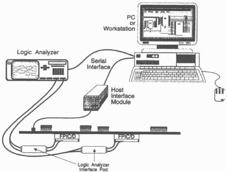
Figure 8–18. The development configuration for system prototyping with the Aptix FPCB Development System.
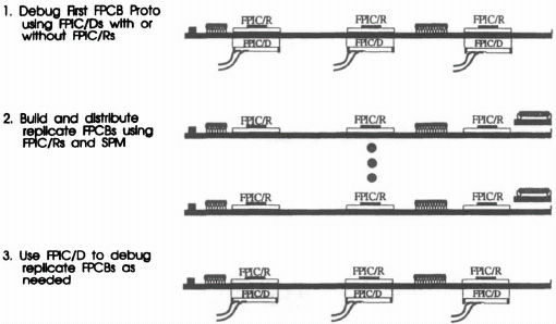
Figure 8–19. The FPIC/D and FPIC/R can be used individually or together depending on the function required.
The Benefits of Programmable Interconnect Today’s system design teams are faced with the conflicting challenges of greater system complexity and shorter development cycles. Aptix FPIC and FPCB provide designers with an effective solution that results in company-wide benefits:
- Instant prototypes from schematic.
- Quick changes allow experimentation/innovation.
- Full signal observability and automated debugging aids.
- Consistent documentation.
- Faster design verification.
- Early system and software integration.
- Quicker time to market.
System and ASIC Prototyping FPIC devices and FPCBs are not limited to component-based system prototyping. They are also quite effective for ASIC prototyping minimizing the time and cost risks associated with such designs. Figure 8–20, for example, shows a typical FPCB-based ASIC prototype using FPGAs for the logic, an FPIC device for the interconnect, and a connector and cable that adapts to a target socket. In this scenario the designer enters the ASIC design, then partitions and maps the logic to the desired FPGA or high-density PLD. The Aptix Development System provides the interconnect routing for the fastest possible performance between FPGAs and the target socket. Since the FPIC device is providing all the pin-to-pin interconnects, the I/O assignments of the FPGAs can be optimized purely for performance, resulting in an even faster ASIC prototype solution. Of course, the FPCB ASIC prototype could actually plug into an FPCB system prototype, thus bringing the benefits of programmable interconnect to the entire design effort.
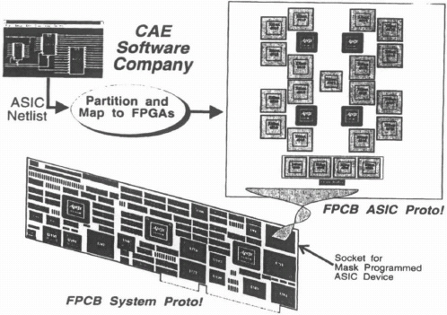
Figure 8–20. The development configuration for ASIC prototyping with the Aptix FPCB Development System.
8.3.2 I-Cube IQ160 Description
I-Cube’s family of field-programmable interconnect devices (FPIDs) is available in a variety of I/O densities, ranging from 96 to 320 usable ports. This family employs a second-generation architecture, resulting in increased performance and architectural flexibility. The FPIDs are manufactured with a 0.8 μ CMOS SRAM process, and are available in a variety of industry standard packaging options.
These devices are designed for use in programmable switching, interfacing, and wiring applications. In switching applications, these devices are used to dynamically switch or multiplex a large number of signals. When used in interfacing applications, FPIDs allow a common board or system to satisfy different interfacing requirements. In wiring applications, these devices emulate a trace on a PCB and can be used to change point-to-point connections between components on a board or signals on the backplane.
At the heart of the FPID is a nonblocking, globally connected crossbar switch, allowing total flexibility in routing signals. Every signal in the crossbar switch can be connected to one or more other signals. Each I/O port is identical and can be programmed as input, output, or bidirectional. The FPID devices support either flowthrough or clocked signal flow. The delays through the devices are identical and predictable, thereby simplifying hardware design.
The crossbar array connections are programmed and the I/O port attributes are configured by storing data in the internal SRAM cells and registers. These devices (Figure 8–21) permit in-system configuration, thereby making them suitable for applications that require static or dynamic (on-the-fly) reconfigurations. Also, they offer two different configuration modes: JTAG-based serial mode for static connections, and a RapidConnect mode for fast configuration changes. The crossbar connections can be programmed incrementally in either mode.
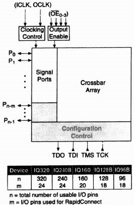
Figure 8–21. Architecture.
The FPID devices support an industry standard JTAG (IEEE 1149.1) interface for board-level testing. A full functional test of these devices can be done using this interface. The same JTAG protocol is used for loading the configuration bit stream into the device in the serial configuration mode.
Architecture External signals pass to each device through its I/O ports. The crossbar switch array is used internally to connect the I/O ports to one another, thereby establishing connections between the external signals.
The JTAG-based configuration controller decodes the incoming configuration bit stream and stores the data into internal SRAM and registers to establish the desired configuration. Additionally, by switching the device to RapidConnect mode, one can directly access the internal crossbar SRAM to make or break crossbar connections incrementally in under 40 ns.
Enhanced Crossbar Array The enhanced crossbar array is an array of pass transistor switches, each programmable with an SRAM cell. Each switch, when programmed to be in the ON state, connects a unique pair of signal lines in the array. The external I/O signals are connected to the lines in the crossbar array.
A connection between two I/O ports is made by closing the transistor switch at the intersection of the crossbar signal lines. The array is globally connected, and therefore a connection can always be made between any two I/O ports. Moreover, only one transistor switch needs to be closed in order to make a connection between two I/O ports. This arrangement provides a nonblocking, architecture offering 100% utilization, guaranteed connections, and uniform and predictable delays.
This enhanced crossbar architecture supports connecting more than two I/O ports together for multicasting/broadcasting operation. A new connection can be made or an existing connection can be broken without affecting other connections, allowing incremental reconfiguration of the crossbar array.
I/O Ports Figure 8–22 shows the general arrangement. The attributes of each I/O port are individually programmable. The attributes include its I/O function, output voltage level, and pull-up current. The various programming attributes are shown in Figure 8–22. Each I/O port is buffered to provide low-capacitive loading (in input mode) and low-impedance and high current drive (in output mode). The I/O buffer is tristatable, using an OutputEnable control signal.
IOB Function: Figure 8–23 shows the different IOB functions that can be programmed and are described in the following section.
Input (IN): In this mode, the external signal at the I/O port pin is connected to the corresponding crossbar line through a buffer.

Figure 8–22. Programmable I/O buffer.
Registered Input (RI): In this mode, the external signal at the I/O port pin is connected to the corresponding crossbar line through a register. The register is controlled by an external clock signal.
Output (OP): In this mode, the corresponding crossbar line is connected to the I/O port pin through a buffer.
Registered Output (RO): In this mode, the corresponding crossbar line is connected to the I/O port pin through a register. The register is controlled by an external clock signal.
Output Force 0 (FO): In this mode, the I/O port pin is forced low (logic 0), regardless of the state of the signal on the corresponding crossbar line.
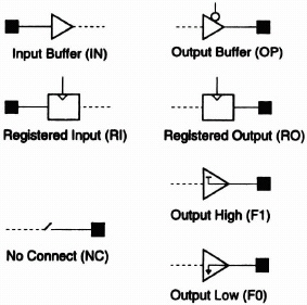
Figure 8–23. IOB attributes.
Output Force 1 (FI): In this mode, the I/O port pin is forced high (logic 1), regardless of the state of the signal on the corresponding crossbar line.
Bus Repeater (BR): This mode is used for connecting two external signals that are bidirectional, but the direction control signal for them is not available. When in this mode, the device automatically detects the driving port and passes the signal to the receiving port. Figure 8–24 shows the circuit.
No Connect (NC): In this mode, the I/O port pin is isolated from the crossbar array.
In the four output (OP, RO, F0, and F1) and the BR modes just described, the active and high impedance states are controlled by the OutputEnable signal.
Output Voltage Level When the I/O port is programmed to be in one of the output modes, the output (high) voltage level can be programmed as transistor-transistor logic (TTL) or CMOS.
Pull-up Current For those I/Os programmed for CMOS output levels, an additional pull-up current of 3 mA or 20 mA can be programmed. The normal pull-up current is 8 mA.
Configuration Control The FPID device is programmed using the JTAG (IEEE 1149.1) serial bus. The JTAG serial bus uses four pins: Test Data In (TDI), Test Data Out (TDO), Test Clock (TCK), and Test Mode Select (TMS). TCK is used to clock data in and out of TDI and TDO. TMS, in conjunction with TDI implements a state machine that controls the various operations of the JTAG protocol. In addition, the reset signal (TRST*) is used to reset the FPID device.
The FPID device, the I/O attributes, and the crossbar connections can be programmed using the JTAG serial bus. Additionally, a special mode called RapidConnect described below in the following subsection, can be enabled or disabled using the JTAG serial bus.

Figure 8–24. Bus repeater.
RapidConnect The RapidConnect mode is used for real-time switching applications, where crossbar connections need to be altered dynamically within the user’s system. In this mode, a designated number of I/O ports are used to directly address the internal crossbar SRAM for writing, allowing contents of the crossbar SRAM to be changed very quickly, resulting in fast connection changes.
Configuring FPID Devices
Bitstream Generation The configuration bitstream generation can be done off-line or in real time in the target system (see Figure 8–25). Software available from I-Cube automates this process.
For applications that do not require FPID devices to be dynamically reconfigured in system, users can generate the required configuration bitstreams offline. The software used for off-line generation accepts a text file describing the desired configuration connections between different I/O ports and functional attributes of each I/O port, and generates a file containing the bitstream. The software guarantees 100% utilization and 100% completion in a single pass. This software is a part of the development system available on PCs and Sun SPARC Workstations.
For applications requiring dynamic reconfiguration of FPID devices, I-Cube offers users a license to C source code libraries and routines. This allows the user to embed I-Cube Development Software into a target system, for in-system, dynamic bitstream generation and downloading (see Figure 8–26).

Figure 8–25. Off-line bitstream generation.
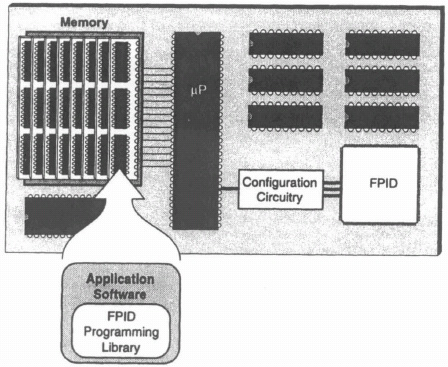
Figure 8–26. Embedded bitstream generation.
Bitstream Downloading The bitstream can be downloaded into the FPID device(s) using several different hardware schemes. The choice depends on the end application. All these schemes use the standard JTAG protocol and timing.
If the target hardware is controlled by a computer such as a PC, the parallel port on the computer can be used to download the bitstream. I-Cube provides a software utility to do this downloading. Under this scheme, the necessary data for TDI and TMS pins as well as the (software generated) TCK clock signal are sent over the parallel port.
An on-board erasable programmable read-only memory (EPROM) or EEPROM, in either bitwide or bytewide configuration, or a serial EPROM can be used to store the bitstream. Using minimal external logic, the bitstream stored in one of these devices can be downloaded into the FPID device(s) over the TDI and TMS pins, with the TCK pin used for synchronization. The clock signal for the TCK pin is generated by the external logic.
If the target system has an on-board microcontroller, the bitstream data can be read from memory (either an EPROM or SRAM) and downloaded into the FPID device(s) using three I/O pins on the microcontroller to generate the required TDI, TMS, and TCK signals. For real-time applications, the microcontroller/microprocessor will generate the bitstream and download it into the FPID device(s) in a single operation.