
4.6 PLACEMENT, ROUTING, AND WIREABILITY
An eternal requirement in CAD tool provision is for automatic place and route, preferably with 100% guaranteed success and with a short run time. Unfortunately, placement and routing takes place within the context of a real design and physical reality imposed by one or more FPGAs, the implementation medium. Any design contains a demand for wires with its point-to-point connections and bus structures. Since the FPGA contains a finite number of wires, all FPGA architectures have a defined wiring capacity. When there are gross discrepancies between the wiring demand of a particular design and the wiring capacity of the target FPGA, it is likely to be difficult to discover an implementation by any method including advanced placement and routing algorithms. It is worth trying to understand the relationship between wiring capacity and demand so that better engineering decisions can be made about the suitability of a particular FPGA for a particular design.

Figure 4–22. Physical designs for the display driver: manual CAL design.
4.6.1 Rent’s Rule and Package Pin-outs
Rent’s rule was originally “discovered" from examining packages of logic modules [Russo71]. It attempts to answer the question, “How many connections (n) are required to a structure holding a number of components (N) each of which has a number of connections (m)?” (see Figure 4–24). The relationship can be stated as n ≈ m * N(l-p), where p is Rent’s coefficient (≈0.5). It has an intuitive explanation if one imagines a square array of components on a board. Cutting the board in half, creating two edge connectors, would expose m![]() wires. The rule can be applied as a “sanity check” on components that deliver random logic, like FPGAs, which are made of N logic cells with m pins contained in packages of n pins. To make the most use of an FPGA while implementing random logic, the ratio of user I/O package pins to connections to the logic cell should be according to Rent. This exercise is left to the reader to be applied to the commercial offerings at any point.
wires. The rule can be applied as a “sanity check” on components that deliver random logic, like FPGAs, which are made of N logic cells with m pins contained in packages of n pins. To make the most use of an FPGA while implementing random logic, the ratio of user I/O package pins to connections to the logic cell should be according to Rent. This exercise is left to the reader to be applied to the commercial offerings at any point.

Figure 4–23. Physical designs for the display driver: LCA design.
4.6.2 Rent’s Rule and Wireability
Heller et al. [Heller78] were the first to attempt an analysis of wiring demand, in this case for logic designs in the context of gate array “images.” They addressed questions such as: What characterizes useful gate array architectures? How big should wiring channels be? What is the average interconnection length of wires? What is the distribution and number of interconnections? Simple one- and two-dimensional models (see Figure 4–25) can be used. This shows three terminal logic elements communicating with a wiring channel of fixed capacity (the capacity in the two-dimensional case is the sum of the horizontal and vertical wiring channels). By using Rent’s rule to compute average wire length and making an assumption on the distribution of wires, it is possible to estimate a channel capacity that will allow the interconnection of a given number of logic elements. This is shown in Figure 4–26. It shows that even for relatively low gate counts, the ideal channel capacity is high, but as the gate count grows logarithmically, the channel capacity grows linearly. The analysis also covers variation for m terminal logic elements. The result indicates that to help the wireability of a design, the FPGA architecture, or structures built from it in the case of channelless arrays, should support channel capacities corresponding to gate count as in Figure 4–26.
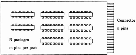
Figure 4–24. Two levels of physical hierarchy.

Figure 4–25. Idealized wiring models.

Figure 4–26. Variation in wire demand with gate count.
4.6.3 Partitioning Designs within and across Chips
Partitioning is important in three areas:
- Partitioning the resources within a single FPGA to support multiple designs
- Partitioning a design into subsystems for placement onto regions of an FPGA
- Partitioning a very large design across more than a single FPGA part
An example of the first case is shown in Figure 4–27. In this case, each of the subsystems is self-contained and can be designed in isolation. There are at least two important design decisions: can the subsystems be fitted onto the chip? and does the pin-out make sense at the board level? It is likely that there is more than one choice of implementation of each subsystem, and that in the parcel packing problem, in laying out the chip, the modules may have alternative shapes. This degree of freedom can be important in making feasible designs. The second question can only be answered in the context of the board design and involves matching the wire demand of the chip pin-out to the wire capacity of the board (defined from the copper dimension design rules and number of interconnect layers).
In the second case the need for partitioning comes from a requirement to divide a large design into subunits for implementation, the traditional divide and conquer approach to engineering problems.
Figure 4–27. Multiple designs on a chip.
PROBLEMS
1. Find a simulator and simulate the display driver design from the logic.
2. Verify Table 4–2 as a correct behavioral description.
3. Verify the same logic block by developing expressions for the outputs evaluating these expressions for the ten binary constant inputs.
4. Simulate the whole design of the stopwatch.
5. Comment on the overpinning or underpinning of some commercial FPGA parts.
6. Describe a wiring strategy for building random logic within a cellular FPGA consistent with wireability rules.
BIBLIOGRAPHY
[Arnold91] Arnold, W., “VHDL makes bid for FPGA designs,” EDN, August 8, 1991.
[Brayton84] Brayton, R. K., Hachtel, G. D., McMullen, C. T., Sangiovanni-Vincentelli, A., Logic Minimization Algorithms for VLSI Synthesis, Kluwer, 1984.
[Bursky92] Bursky, D., “Module Library Seeks Consistency in FPGA Design,” Electronic Design, pp. 31-33, October 1, 1992.
[Egan91] Egan, B. T., “Device-independent Layout Toolset for FPGAs,” Computer Design, p. 117, December 1991.
[Francis91] Francis, R., Rose, J., Vranesic, Z., “Chortle-crf: Fast Technology Mapping for Lookup Table-Based FPGAs,” Proc. 28th ACM/IEEE Design Automation Conference, Association for Computing Machinery, pp. 221-233, 1991.
[Gajski88] Gajski, D. D., Silicon Compilation, Addison-Wesley, 1988.
[Gray79] Gray, J. P., “Introduction to Silicon Compilation,” Proc. 16th Design Automation Conference, pp. 305-306, June 1979.
[Heller78] Heller, W. R., Michail, W. F., Donath, W. E., “Prediction of Wiring Space Requirements for LSI,” Journal of Design Automation and Fault Tolerant Computing, Vol. 2, No. 2, pp. 47-144, 1978.
[Mazor93] Mazor, S., A Guide to VHDL, 2nd ed„ Kluwer, 1993.
[Mead80] Mead, C. A., Conway, L., Introduction to VLSI Design, Addison-Wesley, 1980.
[Naish88] Naish, P., Bishop, P., Designing ASICs, Wiley, 1988.
[Newk83] Newkirk and Mathews, The VLSI Designer’s Library. Addison-Wesley, 1983.
[Russo71] Landman, B. S., Russo, R. L., “On a Pin Versus Block Relationship for Partitions of Logic Graphs,” IEEE Transactions on Computers, Vol. C-20, p. 1469, 1971.
[Small91] Small, C. H., “FPGA Design Methods,” EDN, pp. 114-122, August 5,1991.
[TTL88] The TTL Logic Data Book, Texas Instruments, 1988.
[Weber90] Weber, S., “Here’s a Synthesizer that Supports VHDL,” Electronics, April 1990.
[Weste93] Weste, N., Eshragian, K., Principles of CMOS VLSI Design, Addison- Wesley, 1993.