
4.3 DESIGN PROCESS FLOW: THE PROGRAMMABLE LOGIC DEVICE ROUTE
A typical programmable logic device (PLD) design process flow is shown in Figure 4–6. The starting specification might be informal and hand drafted in anything from an HDL to a collection of Boolean equations. Design capture moves the design into the CAD environment and requires the engineer to restate the creation for machine consumption. This might be preparing a file in a preferred notation or marking entries in a table. Synthesis and optimization uses algorithms to manipulate the logic design to improve it by exploiting don’t care states to minimize the number of gates used. Function verification may be a unit-delay simulator to generate circuit outputs, or may amount to a manual inspection of truth table data. Device fitting matches logic/gate demand and input/output (I/O) demand to part family members. Finally, physical design produces manufacturing data, a binary stream, for programming specific devices. This must be achieved by generating a layout of the required circuit in the chosen FPGA cell and wire scheme. It may amount to running a simple logic block generator or it may be placing and routing random logic using manual and automatic software tools.
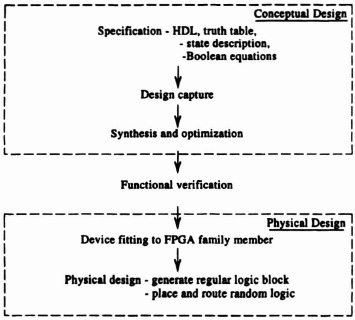
Figure 4–6. PLD design process flow.
4.3.1 Conceptual Design of Display Driver
In the case of a CAL design the specification is given in Table 4–2. The minimization of this table using ESPRESSO [Brayton84] is shown in Table 4–3. Now this is a standard sum-of-products form that we can expect to implement within an array of cells that allows a two-level logic structure to be built.
In the case of the LCA implementation, because there is no “natural” form for implementing a two-level logic structure, designs must be created as fully instantiated (flat) netlists. For the display driver design specified in the PALASM2 of Figure 4–3, a netlist must be optimized by proprietary tools to accommodate implementation in configurable logic blocks (CLBs) and the result merged with a top-level schematic to create the complete design.
4.3.2 Design Verification of Display Driver
In the case of the CAL design, since the logic was synthesized there is no formal verification step other than informal inspection of the truth tables.
In the case of the LCA design, the flat netlist of logic primitives can be exercised with a logic simulator. The result of this for a test pattern of the ten digits is shown in Figure 4–7. Readers can manually construct the digits from the output to confirm the correct functions are being computed.
4.3.3 Physical Design of Display Driver
In the case of the LCA implementation, the result of applying placement and routing algorithms to the merged netlist is shown in Figure 4–23.
In the case of the CAL implementation, physical design can be automatic, as in the synthesized ROM logic block of Figure 4–21, or physical design can be place and route (manual or automatic) from a suitable gate-level netlist. Using the gate-level schematic of Figure 4–4 yields the manual design shown in Figure 4–22. The synthesized ROM is further described in Section 4.5.1. It is interesting to compare the quality of the logic synthesis with that of a manual implementation generated with software design tools. The configurable logic ROM implementation requires an 11 (4 inputs plus 7 outputs)-by-8 (product terms) array of cells compared with an ll-by-4 array when implemented by hand. The following points are worth noting:
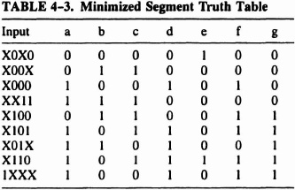

Figure 4–7. Result of simulating display driver.
- Flexibility. The greatest advantage of the human-generated implementation is the way the layout of the logic unit has been optimized to fit in with the chip pin-out requirements and the counter design. Although there is a structure to the layout (note that input variables are routed horizontally across the array and outputs are collected using vertical wires), it is specific to this particular example.
- Variable Ordering. In the automatically-generated array the order of the input variables in the cascade of gates is fixed. Only the function performed by gates in the cascade can be changed. The human implementation achieves a much better factorization of the logic equations by changing the order of variables in the gate cascades and using trees rather than simple cascades of gates. This can only be achieved by having a special routing plan for each function implemented.
- Design Time. Although the automatic implementation is much less efficient, it only took about 10 minutes. The human-generated implementation took several days.
- Design Size. This example approaches the limit of the size of circuit which may be designed efficiently by a person, and at this level of complexity, human design may surpass automatic design. But for the most part circuit optimization can be left to algorithmic methods.