
3.6 PROGRAMMING
3.6.1 Technology
The main technologies used in the control store of FPGAs and programmable logic devices (PLDs) are as follows.
Static RAM The basic static RAM cell consists of two CMOS inverters connected in a loop to form a bistable device. The state of this device can be overwritten by external signals on the bit lines (marked B in Figures 3-18 and 3-19) via pass devices gated by the word lines (marked W). The sizes of the transistors are chosen to ensure that normal logic values on the bit lines can change the state of the cell (write cycle), but if an intermediate voltage is placed on the bit line, which is then left floating, the RAM cell itself can drive the bit line high or low according to its state (read cycle). In the case of the six-transistor RAM (Figure 3–18) true and complement values are applied to both sides of the RAM (effectively pushing and pulling it during a write), and in the five-transistor RAM (Figure 3–19) only one signal is applied (push only). Five-transistor RAMs are significantly more dense than six-transistor RAMs because less area is required to route bit and word lines through the array: they are also much harder to design and have less noise immunity. As process technology moves below 1 μm and with the move to 3-V power supplies, five-transistor RAM designs are being replaced by the more stable six-transistor cells.
The RAM cell is a storage device only, and in the FPGA application its Q output will control a separate (normally n-type) transistor switch.
EPROM The EPROM device is based on special metal-oxide semiconductor field-effect transistors (MOSFETs) with floating (unconnected) gates (Figure 3-20). If sufficient charge is trapped on the gate, the channel will conduct. Thus the EPROM transistor can function as a simple switch in the same way as a fuse or antifuse. Charge is injected into the silicon dioxide above the transistor channel in a special programming mode by generating high-energy “hot” electrons within the channel region using higher-than-normal voltages. These electrons are attracted toward the floating gate by capacitive coupling. When the high programming voltage is removed, the electrons are trapped in the floating gate. Ultraviolet light is used to erase the device by giving the trapped electrons sufficient energy to escape from the gate dielectric. Programming and erasing of EPROM-based devices normally take place outside the target system and require special equipment. In addition, erasing devices is a relatively slow process, taking about 15 to 20 minutes.
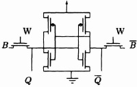
Figure 3–18. Six-transistor static RAM.

Figure 3–19. Five-transistor static RAM.
EEPROM The electrically-erasable programmable ROM (EEPROM) transistor (Figure 3–21) is similar to the EPROM transistor, but a second polysilicon gate overlapping the first floating gate is added. EEPROM devices are erased electrically by applying a suitable voltage to this second gate to allow electrons trapped on the floating gate to be discharged by a tunneling mechanism. EEPROM cells are somewhat less dense than EPROM cells and to date have found application only in relatively simple (GAL) Generic Array Logic devices which are reprogrammable pin equivalents for PALs. GALs are normally programmed out of circuit using special equipment. Most EEPROM technologies have a limit on the number of read/write cycles before the device fails: this limit makes the technology unsuitable for use in computational applications where the device may be reprogrammed thousands of times.

Figure 3–20. EPROM floating-gate MOSFET. Reprinted with permission of McGraw-Hill from Geiger, R. et al. “VLSI Design Techniques for Analog and Digital Circuits,” McGraw-Hill © 1990.
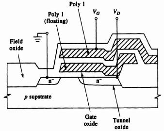
Figure 3–21. EEPROM floating gate MOSFET. Reprinted with permission of McGraw-Hill from Geiger, R. et al. “VLSI Design Techniques for Analog and Digital Circuits.” McGraw-Hill © 1990.
Fuse This technology relies on simple fuses formed from metal links that are forced open circuit by high programming currents. Since the fuses are made of metal they have low impedance in the closed condition and hence can support high-speed operation. Fuses are used on most low-density PAL devices based on bipolar technology: they are not found on any high-density FPGA- type devices. Current technology can guarantee a programming yield of about 97% for fuse-based devices, that is, 3% of devices supplied to customers can be expected not to program correctly.
Antifuse An antifuse is a two-terminal circuit element that normally offers a high impedance between its terminals, but after a programming voltage higher than the operating voltage is applied, the impedance is reduced to a low value permanently. This is the opposite behavior to a fuse where the programming voltage causes the device to enter a high impedance state. Normally-open antifuses are more suitable than fuses for use in gate-array-like structures because the metal segments and logic resources of the device can be tested in isolation before any antifuses are programmed. Another advantage is that antifuses are blown where connections are required on the user design, whereas fuses are blown wherever a potential connection provided by the underlying architecture is not required: this implies that in a general-purpose device far fewer antifuses need to be programmed than fuses. There are several antifuse structures in use, of which the most popular is the programmable low-impedance circuit element (PLICE) used in Actel gate arrays (Figure 3–22). When an 18-V programming pulse is applied across the terminals (drawing a current of 10 mA for less than 10 ms) the dielectric is ruptured and the device impedance is reduced from a value above 100 MΩ to a value less than 1 kΩ. These values are guaranteed by the manufacturer. The PLICE antifuse is bidirectional in its low-impedance state. Another important criterion for antifuse-based devices is the range of maximum and minimum resistances within which an antifuse is said to be programmed. Adaptive programming techniques are utilized to program antifuses to final resistances with minimum variations.
Other technologies such as ferric RAM and flash EPROM may be expected to be used in this application in the near future.
3.6.2 Issues
The different classes of FPGA device have different goals and requirements for their programming interface. In the ASIC replacement application, for example, simple low overhead interfaces are required (a real ASIC has no programming overhead), whereas the computational array requires a high bandwidth interface to support rapid reprogramming. The main issues in the choice of programming interface and control store technology are discussed in the following sections.
Overhead Pins Overhead pins to support programming in RAM-programmed FPGAs increase package and hence part costs. Extra data and address busses are expensive at the board level. However, they allow random access to the control store for rapid reconfiguration and access to the state within the user logic. In some devices, programming and device I/O signals share a physical pad, with a mode control input to select which is active. One disadvantage of this scheme is that if the configuration of the device needs to use the shared I/O pins, control store accesses cannot be made without affecting the computation being implemented by the device.

Figure 3–22. PLICE antifuse, (© Actel Corporation, 1993. All rights reserved.)
External Support Circuitry With RAM-programmed FPGAs it is necessary to load the device configuration into the RAM control store from external nonvolatile storage, normally EPROM or ROM. It is desirable that this is done with the minimum of support chips: there is not much point in replacing ten TTL and PAL devices with an FPGA if one needs four TTL devices and an EPROM to bootstrap the FPGA! Thus placing the bootstrap logic on the FPGA itself is highly desirable in stand-alone applications. On the other hand, when the FPGA is to be used in a microprocessor-based system, a straightforward memory-like interface can be attractive; depending on the function of the FPGA, it may be possible for the microprocessor or microcontroller to load its configuration from the system's nonvolatile storage. It is also desirable that when multiple FPGAs are used on a board they can be configured from a single large memory and associated circuits, rather than multiple smaller memories and associated circuits for each FPGA.
Testability The choice of programming method affects testability of systems using FPGAs in several ways. Use of RAM-based rapidly reprogrammable FPGAs allows special FPGA configurations to be developed for use in system tests. These can be used to test board traces and even adjacent non-FPGA devices as well as the FPGA chips themselves. This technique has the potential to reduce test time for completed assemblies and the need for complex board testers and to allow self-test in the field. This method of testing using FPGAs can be successfully integrated with the JTAG boundary-scan methodology. Note that the reconfigurability of FPGAs allows a special configuration for board testing and can make it unnecessary for the FPGA to provide dedicated hardware resources for JTAG registers. Conversely, use of write-once technologies such as antifuse has adverse implications for tests, in that the configurations of the devices themselves must be verified. In general, it is not always sufficient to rely on the device programmer to check that fuses read back correctly since a partially blown fuse may pass a static read back test but cause the device to fail at operating speed and temperature.
Reliability There are reliability concerns associated with the configuration store of all FPGA technologies.
Write-once fuse-based devices such as PALs can be sensitive to the calibration of the programming equipment. Pin-equivalent devices from different manufacturers often have different programming algorithms. Failure to observe the manufacturer's specifications exactly may cause higher numbers of devices to fail on the programmer, but more seriously, devices may pass the programmer read back test but fail in the field. Such failures can be intermittent and are often hard to diagnose. It is essential that devices are programmed on a trusted system and that the programmer is well maintained. When this is done field failures are rare although a significant percentage of devices may fail to program correctly—there is no way for a PLD manufacturer to test if a fuse will fuse before it leaves the factory. Another concern for some programming technologies in safety-critical applications is that they have not been in production long enough to verify their long-term reliability. It is impossible to say for certain what percentage of devices will survive ten years when they have only been manufactured for three, although accelerated failure tests can provide enough confidence for most applications.
The reliability concerns with RAM-programmed technologies are centered around well-known effects experienced with commercial SRAM devices. The most serious problem is that alpha-particle radiation can potentially change the state of one of the control RAM cells. This is called a soft error, since the state of the RAM can be restored by writing it again. Extreme doses of radiation can cause unrecoverable failures in all common VLSI technologies, although different technologies have different degrees of radiation hardness. Failures are less likely to occur on FPGAs than normal SRAMs because FPGA RAM cells normally have a higher load capacitance (because they are connected to logic), are accessed relatively rarely (RAM cells are at their most vulnerable to spurious writes during a read cycle when internal voltages are compromised), have better power supply connections (RAM designers can take advantage of the low power consumption of static RAM cells to route power locally on nonmetal layers, whereas FPGA designers will normally route on wide metal tracks to support adjacent logic circuits), and are designed for stability rather than access speed. Choice of packaging technology can also reduce the radiation problem since alpha particles are emitted by the package: plastic packages emit at a rate about ten times lower than ceramic packages. An analysis of the soft error rate caused by this mechanism, based on experiments with radioactive sources placed in direct contact with the die to accelerate soft error rates predicted that a Xilinx XC2064 device would function for about 46,000 years without an error under normal conditions. Similar results are likely for the other SRAM-programmed parts since the memory cells are of the same basic design. As process technology improves and transistor sizes become smaller, RAM cells will become more sensitive to alpha particles. There will be more of them per device, and so the soft error rate is likely to increase.
Although it is impossible in theory to stop soft errors from happening, they can be detected by reading back the control store and comparing against a reference or using parity or other error-detection codes. Checking circuits can be built into devices or be external, as are the parity checkers for computer memory chips. The value of such checking circuits is open to question given the inherent reliability of the static RAM technology used in FPGAs compared to that of the dynamic RAM (DRAM) technology where parity checking is normally applied, the much smaller number of bits of store involved, and the fact that the action of reading the RAM itself could have a negative impact on device reliability. Another approach would be simply to refresh the control store periodically without attempting to determine whether errors had occurred. For some designs, this can be done without disturbing the current computation. This approach has the merit of avoiding the need to read the device control store during operation.
It should also be noted in this connection that soft errors can potentially occur on any bit of state in a digital circuit in all common implementation technologies, including the state of the user's design. Since there are likely to be much fewer bits of state in the user's design than in the configuration store and the structures involved are physically larger than those in a RAM cell, it is much less likely to happen there. Thus it could be argued that if soft errors are of concern in a particular application, it would be more appropriate to use a self-checking design style (e.g., triplication) within the design implemented on the FPGA than to check the FPGA's control store. Such design styles also detect errors immediately and can often compensate for them or fail gracefully; parity checking the control store can do no more than raise a flag that something went wrong at some time in the past after incorrect results have been output.
EPROM-based technologies are sensitive to the device the programmer used, as are all fuse-programmed devices. In addition they can be erased by UV light: manufacturer's data gives a figure of about 1 week of exposure to direct sunlight or 3 years exposure to fluorescent room lighting to erase an EPROM if a suitable opaque label has not been fitted. In the context of device reliability we are more concerned with the exposure required to make it probable that a single bit will be erased rather than the time to erase the whole device. Versions of EPROM-based erasable programmable logic devices (EPLDs) in nonwindowed packages are worth considering for high-reliability applications. Given their sensitivity to UV light, use of these devices in environments where they might be exposed to other forms of radiation (e.g., X-Rays) should be considered carefully.
Technologies based on electrically erasable memory may be unreliable if exposed to either radiation or voltage transients on programming pins.
All the programming technologies used in FPGA devices to date have more than adequate reliability for most applications. When considering FPGAs for safety-critical applications or stressful environments it is important to make a thorough study of the reliability of the chosen device. This may involve persuading manufacturers to release proprietary information or running one's own characterization experiments on the device.
Manufacturing Concerns There are several manufacturing concerns related to the use of write-once FPGA devices: RAM-based devices present no special difficulties. The most obvious concern is that the devices must be programmed during manufacture. This has several consequences.
- Some devices will fail to program correctly: this must be taken account of in price comparisons between technologies and in determining inventory levels.
- Programming the FPGA devices is an additional manufacturing step that must be coordinated with the others and requires its own tooling, which can be relatively expensive. Most complex FPGA antifuse-based devices take a significant amount of time to program and some require that user-supplied test vectors be run.
- It may be necessary to swap PLDs in the field after design revisions or after a completed board fails the final test. Therefore, it is common practice to use sockets with write-once PLD devices, while other components are normally soldered directly to the board. The cost of sockets can be significant in volume manufacture, and sockets themselves compromise reliability by making the assembly more susceptible to mechanical shocks. If you do not believe this then try mailing a few boards with socketed PLDs overseas! Sockets also involve an extra assembly stage in which the components are inserted; failures can be introduced here by poor connections between device pins and sockets (especially on high pin count devices) and device leads that bend under the device rather than entering the socket (especially dual-in-line (DIL) devices).
- The fine lead pitch on high pin count surface mount packages can cause handling problems with devices that are programmed out of circuit. The process of inserting and removing the device from the programmer socket may displace one or more leads sufficiently to cause problems when the device is mounted on the board. For this reason, it is likely that in-circuit programming will become the technology of choice for high pin-out devices.
Granularity and Speed of Reconfiguration Granularity refers to the smallest unit of the FPGA that can be reprogrammed. In most cases this is the entire chip. Allowing small changes to the configuration RAM allows dynamic reconfiguration of subcircuits and can be attractive in computational applications. This feature can be used to set the state of latches in the design implemented on the FPGA. This feature is attractive even in logic replacement applications since it can dramatically simplify the circuit to be implemented on the FPGA, for example, by eliminating the need for load and clear functions on a counter.
Access to Internal State Access to internal state is desirable to support design debugging and in computational applications to access results without the overhead of routing them to the edge of the array. There are two main techniques for providing such access:
- Special output lines, which can be selectively connected to the outputs of internal gates and are available at dedicated pads. This technique allows real-time monitoring of internal signals using conventional test equipment and is very useful for debugging FPGA designs embedded in board-level systems. Normally there are a very small number of such lines available, so relatively few circuit nodes can be monitored. This technique is used in the “actionprobes” of Actel's FPGAs that allow two internal device nodes to be monitored in real time.
- Mapping cell outputs to control store RAM. This technique is most useful in devices that allow random access to the control store. Although signals cannot be monitored in real time, any node in the circuit can be watched and no external test equipment is required. This technique is particularly advantageous in computational applications where the clock to the user circuit can be controlled by the host computer performing the accesses to memory. This technique is used in the Algotronix CAL applications.
Design Security Many write-once PLDs have a “security” fuse which when blown, prevents the fuse array from being read back by a device programmer. This feature is intended to prevent competitors from “reverse engineering" the user design, that is, determining the principles of operation. Naturally, it also has adverse consequences for testability and diagnosis of failures in the field. The security fuse on simple PLDs is of no value because the configuration can easily be determined by applying vectors to the device pins. With most complex PLDs based on a PAL architecture, the security fuse would be little more than an inconvenience to the determined. Less obviously, RAM-programmed FPGAs can give design security since the contents of their control store is lost when power is removed. When RAM-programmed FPGAs are used in conjunction with a host microprocessor, extremely secure operation is possible since encryption can be used to protect configurations prior to downloading into the FPGA (configurations for the FPGA can come into a tamperproof module over a communications interface, and so need not be present in nonvolatile store within the tamperproof unit) and the microprocessor can rapidly overwrite the control store or remove power to the FPGA if it detects attempts at tampering.