
4.4 DESIGN PROCESS FLOW: THE APPLICATION-SPECIFIC INTEGRATED CIRCUIT ROUTE
There are many sources of ASIC design process flows. VLSI design methodologies [Mead80], [Weste93] and ASIC manufacturers [Naish88] are good sources. The former place greater emphasis on layout issues, such as wiring management, to achieve optimal physical designs, while the latter largely rely on structural design to manage the whole process flow. A generic model for ASIC process flow is shown in Figure 4–8. Both the Gajski-Kuhn and more traditional forms are shown. This indicates the refinement of a specification to a structural design before entering design validation and physical design processes. In reality the behavioral and structural descriptions are built by stepwise refinement of the design. A typical ASIC design process flow, represented by paths in the Gajski-Kuhn diagram, shows the three design descriptions being built and the grain of the design unit decreasing. Thus a starting behavioral specification posits a structural design. This could be a composition of interconnected function units. This, in turn, could be stepwise refined by expanding to a structural design of simple elements, a gate-level netlist, or synthesizing a two-level logic block.
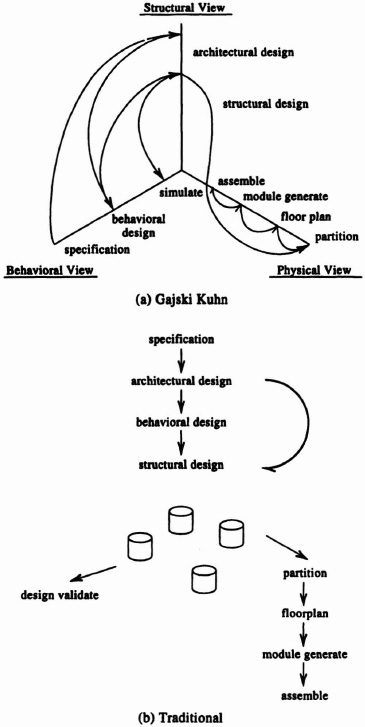
Figure 4–8. ASIC design process flow.
To illustrate the flow let us return to the display driver example. In fact, the 7-segment display driver was part of a larger timer design exercise for a VLSI course. It had the specification: Design a simple stopwatch to count in tenths of a second to one minute and display the current time on three 7-segment displays (tenths, seconds, and tens of seconds). The watch is controlled by three signals: INIT clears the watch and puts it in the “stop” state, SS start/stop is a high-going edge to start the watch from the stop state (a high-going edge in the start state puts the watch in the stop state), CLOCK, a 10-Hz signal.
4.4.1 Conceptual Design of Stopwatch
The 7-segment decoders provide a good example of “random” combinational logic, while the counters provide a good example of classic sequential logic. This design uses three separate units for the three displays although the design complexity and area could be reduced by implementing it as a single-state machine with multiplexed displays (since the large 7-segment decoder logic would not need to be duplicated). This is necessary to comply with the design specification given.
The Counter The counter is built from four toggle flip-flops (Figure 4–9). The basic 4-bit ripple counter is converted to a decade counter by a gate that sets the clear line when the counter gets to ten. The output of this gate is also used as the clock for the succeeding counter. The counter can also be cleared by the user’s INIT signal. Providing the clear capability is the only real problem in the design of the toggle flip-flop (the basic D latches have only clock and D inputs). The clear is provided by extra logic gates that force Os onto the D inputs and 1s onto the clock inputs. A basic master-slave flip-flop can be built with only two D latch cells, whereas this clearable implementation requires six cells. The layout is shown in Figure 4–10.
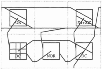
Figure 4–9. Toggle flip-flop design.
The Decoder The decoder takes advantage of the ability to produce any function of two Boolean variables within one cell and uses three levels of logic rather than the two-level logic normally used to implement such functions. Its schematic description is given in Figure 4–4 and physical design in Figure 4–22 later.
The Control Logic The controller function (at the bottom left of Figure 4–11) is implemented using a toggle flip-flop. The design is the same as those within the counters. The toggle flip-flop is clocked by the start-stop input and its output determines whether the counter should be stopped or run freely. The initialize signal clears the control flip-flop and stops the counter. The counters are stopped by ANDing the 10-Hz clock with the output of the control flipflop: thus when the output of the control flipflop is 0, the counters clock inputs are held low, and when it is 1 the counters receive the 10-Hz clock input.

Figure 4–10. Counter design.
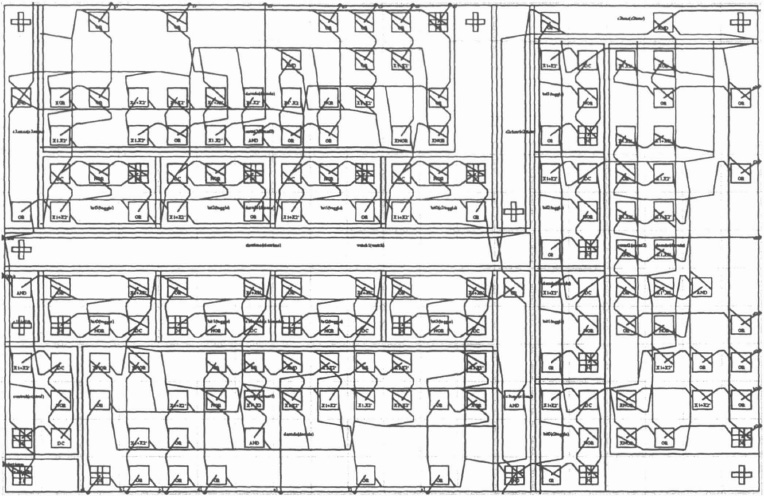
Figure 4–11. Full Stopwatch design.

Figure 4–12. Stopwatch floorplan.
4.4.2 Design Verification of Stopwatch
See Problem 3.
4.4.3 Physical Design of Stopwatch
The floorplan of the full watch circuit is given below as Figure 4–12 and the layout in Figure 4–11. The floorplan is based on using three sides of the design to make connections to each of the displays accessible and the fourth side to get the control signals into the chip. Note that the floorplan requires simple transformations, rotations, and mirroring of the basic unit.