
6.8 A FIELD-PROGRAMMABLE GATE ARRAY FOR SYSTOLIC COMPUTING
6.8.1 Introduction
Recent work [Gray89] [Gokhale91] [Bertin92] has shown that a handful of SRAM-based field-programmable gate arrays (FPGAs) wired together can achieve extraordinary levels of performance, often outperforming supercomputers at a tiny fraction of the cost. And, unlike ASIC solutions, these systems are general purpose and reprogrammable: they can be reconfigured in milliseconds to perform a completely new task.
The CLi6000 series of SRAM FPGA’s from Concurrent Logic has evolved through several generations and is the product of two joint-development efforts, with Apple Computer [Furtek90] and National Semiconductor [Furtek92]. The original motivation for the technology, and still a key application area, is the acceleration of compute-intensive algorithms by exploiting the parallelism inherent in hardware. The capabilities of the technology are illustrated through a massively parallel algorithm for performing motion estimation, an especially compute-intensive algorithm used in digital video compression. The algorithm which determines the best estimate of how blocks of pixels move from frame to frame requires about 4,000 MIPS to perform in real time on a standard video signal.
The algorithm is implemented as a systolic array of 256 processing elements, each achieving 100% efficiency with no wasted clock cycles through pipelining, and a clever synchronization of input pixel streams. The CLi6000’s high register count, NAND/XOR cell states, multiplexer states, fine-grained architecture, array symmetry, and high cell connectivity all work together in efficiently implementing the heavily pipelined, bit-serial arithmetic operations used in each processing element.
6.8.2 CLi6000 Architecture
At the heart of the CLi6000 architecture* is a symmetrical array of identical cells (Figure 6–45). Routing within the array is either by bus or by direct connection between neighboring cells (Figure 6–46). Direct connections are most useful in tight spaces and over short distances where maximum flexibility is required. Busses support fast, efficient communication over longer distances.
There are two kinds of busses: local and express. Local busses are the link between the array of cells and the bussing network. Express busses are not connected directly to cells and hence provide higher speeds. Connective units, called repeaters, spaced every eight cells, divide each bus both local and express into segments spanning eight cells. Repeaters can: isolate bus segments, connect local-bus segments, connect express-bus segments and provide local–express transfers.
The cell (Figure 6–47) is simple and small and yet provides many important and commonly used logic functions, including those most useful in pipelining and arithmetic: a D-type register, a NAND/XOR pair and a two-input multiplexer. The register is essential in pipelining, which is the most effective way to achieve high system throughput. The high register count of the CLi6000 architecture (there are 3,136 in the CLi6005) makes pipelining simple and efficient. The NAND and XOR, available simultaneously in a single cell, provide efficient implementation of full adders and other arithmetic functions. The multiplexer, available by itself or feeding into a register, finds many uses in a broad range of circuits.
Figure 6–45. CLi6000 array (10 × 10 Section).
Because its four sides are functionally identical, each cell is completely symmetrical. Cell symmetry together with array symmetry, high cell connectivity, and a fine-grained architecture make the design of hard macros (circuits with fixed layouts) especially easy. More specifically, it facilitates the creation of bit-slice macros, hard macros in which the inputs/outputs on one side are aligned with the outputs/inputs on the opposite side. A larger circuit is constructed by simply abutting these bit-slice macros. The remainder of this section describes just such an approach in implementing a massively parallel algorithm.
6.8.3 Motion Estimation
Motion estimation is concerned with finding the best estimate of how blocks of pixels move from frame to frame in a video signal. For a block of pixels in the current frame (the current block), the object is to find the best match among search blocks the same size within a search window of the preceding frame. The best match is determined by finding the minimal error (distortion) between the current block and the search blocks. For a block C in the current frame and a block P in the preceding frame:
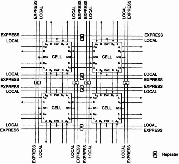
Figure 6–46. Cell connections.
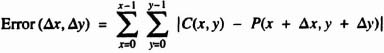
where x and y are the horizontal and vertical displacements, respectively, of the search block relative to the current block, and X and Y are the horizontal and vertical dimensions, respectively, of the blocks being compared. The motion estimation algorithm returns both the displacement vector x, y and Error(x, y) of the best match. This calculation is repeated for each block in the current frame, which is assumed to be tiled with blocks except for an indentation around the edges to allow for the displacement of search blocks.
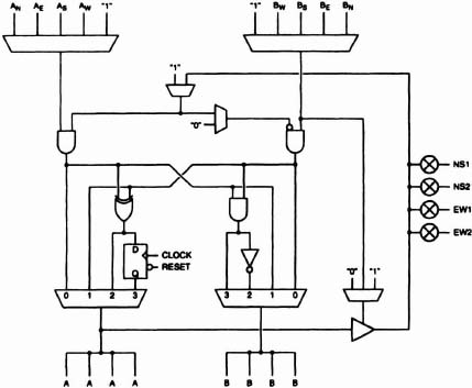
Figure 6–47. Cell structure.
We assume a standard video signal:
Frame rate: 30 frames/sec
Frame size: 360 pixels × 288 pixels
Pixel depth: 8 bits
Block size: 16 pixels × 16 pixels
Max hor. displ: −8, +7
Max vert, displ: −8, +7
The frame rate and frame size lead to a pixel rate of 3.11 MHz, which, in the bit-serial algorithm described here, means a bit rate and clock frequency of 24.88 MHz.
The algorithm assumes four bit-serial inputs:
- Preceding Frame: Upper Band
- Preceding Frame: Lower Band
- Current Frame
- Start of Block
The ordering of pixels in the first three inputs is by horizontal bands. Each band is 16 pixels high, and the pixels within a band enter serially by column, from top to bottom (Figure 6–48). The two bands in the preceding frame straddle the band in the current frame. The Upper Band is offset from the current band by 8 pixels, while the Lower Band is offset by +8 pixels. The scanning of all three bands starts at the same time.
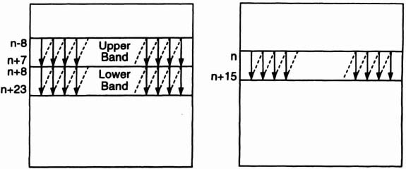
Figure 6–48. Input ordering: (a) preceding frame; (b) current frame.
Start of Block (SOB) signals the start of a new 16 pixel × 16 pixel block in the current frame. SOB is assumed to be active high, a high value coinciding with the first (8-bit) pixel of the new block. The first 16 × 16 block in a band of the current frame is indented by 8 columns to permit search blocks to be displaced by 8 pixels (Figure 6–49). Thereafter, blocks arrive every 16 columns. (In the algorithm described below, blocks need not abut, but they must not overlap.) Figure 6–50 illustrates the search window, containing 256 search blocks, corresponding to the current block. (The search window does not reach the bottom of the Lower Band because search blocks are displaced a maximum of +7 pixels.)
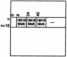
Figure 6–49. 16 × 16 block in the current frame.
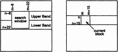
Figure 6–50. Current block and corresponding search window: (a) preceding frame, (b) current frame.
6.8.4 Algorithm Overview
The algorithm is bit serial and massively parallel. Figure 6–51. is a block diagram showing the heart of the algorithm: a linear array of 256 processing elements (PE’s). The array, as well as each PE, has nine inputs:
- Current_Frame (CF)
- Select_Upper_Band (SUB)
- Select_Lower_Band (SLB)
- Upper_Band (UB)
- Lower Band (LB)
- Start_Of_Block (SOB)
- End_Of_Block (EOB)
- Error_Low_Order_Byte (ELOB)
- Error_High_Order_Byte (EHOB)
The Current-Frame pixel stream is supplied directly to the CF input of the linear array. The Upper-Band pixel stream, however, is delayed by 1024 clock cycles before being supplied to the UB array input. The delay retards the Upper-Band pixels by 8 columns relative to the current frame. (8 columns × 16 pixels/column × 8 cycles/pixel = 1024 cycles) The Lower-Band input is delayed by 1152 clock cycles, which retards the Lower-Band pixels by 9 columns relative to the current frame. (9 columns × 16 pixels/column × 8 cycles/pixel = 1152 cycles) Clock Gen provides an 8-cycle high value every 128 clock cycles to both the SUB and SLB inputs of the array. Start of Block synchronizes Clock Gen so that this high value coincides with the first pixel of each column on the CF, UB, and LB inputs. Start of Block is also fed directly to the SOB input and is delayed by 2040 clock cycles to provide the EOB input. The values on the ERL and ERH inputs are immaterial since they are replaced by PE-supplied values. ERL and ERH are arbitrarily set to “0.”
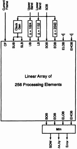
Figure 6–51. Block diagram of motion-estimation algorithm.
The array outputs SOB and EOB are each delayed by 2304 (9 × 256) clock cycles from the corresponding inputs. The 256 errors associated with the 256 search blocks appear serially on the ELOB and EHOB outputs. Min looks for the minimal error and supplies that error along with the corresponding displacement vector.
6.8.5 Processing Elements
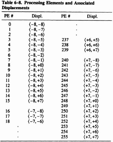
Each processing element has nine outputs to match its nine inputs. The array of 256 PE’s is formed by connecting the outputs of one PE to the matching inputs of the next PE, as shown in Figure 6–52. The computational demands of motion estimation are handled through massive parallelism: each PE computes the error between the current block and one of the 256 search blocks. Table 6-8 shows the correspondence between PE’s and displacement vectors.
There are actually two slightly different types of processing elements: the one in Figure 6–53 is used for all PE’s except for PE 0 and every 16th processing element thereafter that is, for all PE’s except PE 0, PE 16, PE 32, PE 48, PE 64, .… These PE’s are identical to the one in Figure 6–53 except that the SR latch and associated multiplexer are omitted, and just Upper-Band pixels are fed to the absolute-difference module.
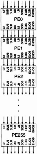
Figure 6–52. Array of 256 processing elements.
At the heart of both types of processing elements is an absolute-difference module and an accumulator. The circuitry to the left supplies the absolute-difference module with two bit-serial streams of pixels. The circuitry to the right resets the accumulator at the beginning of a new block, and at the end of the block places the accumulated error both high- and low-order bytes† on busses that transport the values to the end of the PE array.
The left-side circuitry assures that the proper pixels for the current block and search block are supplied to the absolute-difference module. There is no problem with the current-block pixels they are constant for all PE’s. The search-block pixels, however, must be synthesized from the Upper- and Lower-Band pixels. The key to making this happen is the fast-track/slow-track technique pioneered by Dick Lyon in his serial multiplier designs (see Lyon [Lyon76] and Denyer & Renshaw [Denyer85]). The SLB, UB and LB signals are on fast tracks 0 clock-cycle delay per PE while the CF and SUB signals are on slow tracks 8 clock-cycle delay per PE.
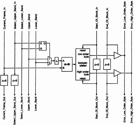
Figure 6–53. Processing element N(N ≠ mod 16).
To understand how the circuitry works, consider the pixel-alignments entering PE 0. The pixels in the Synthesized band, which are identical to the Upper-Band (UB) pixels, are displaced by 〈 −8, −8〉 relative to the Current (CF) pixels. ‡ This is consistent with Table 6–8, which indicates a displacement of 〈−8, −8〉 for PE 0.
Now consider the pixels entering PE 1. Because of the 8-clock-cycle delays on the Current Frame and the Select_Upper_Band (SUB) signal, the Upper and Lower Bands and the Select-Lower-Band (SLB) signal have been advanced by one pixel (8 clock cycles) relative to the Current pixels and SUB. SUB, which is always aligned with the Current pixels, sets the SR latch at the beginning of each new column of Current pixels. Setting the latch causes the Synthesized pixels to come from the Upper-Band until the latch is reset by SLB. SLB, which is coincident with SUB entering PE 0, is advanced by one pixel relative to SUB entering PE 1. The Synthesized Band therefore, takes only the 16th (last) pixel in each column from the Lower Band. The result of all this is that the Synthesized pixels are now displaced by 〈−8, −7〉 relative to the Current pixels. In other words, the search block has dropped down one row. This pattern continues for PE 2 through PE 15, with each succeeding PE adding a row of pixels from the lower band.
The pattern is broken for PE 16 because we no longer want to move down one row but rather back to the top of the search window and to the right one column. This is accomplished by eliminating the Upper-Band/Lower-Band multiplexing logic, and simply reverting to the upper band. The pattern described above for PE’s 0-15 now repeats for PE’s 16-31, and for every succeeding group of 16 PE’s.
On the right side of Figure 6–53, we again employ the fast-track/slow-track technique. The SOB and EOB signals are on slow tracks 8 clock cycles delay per PE to match the speed of the CF signal on the left side. The ELOB and EHOB signals are on fast tracks 0 clock cycles delay per PE so that the two errors from each PE fill unique slots.
The SOB signal is timed so that the low- and high-order registers in the accumulator are reset just as a new block begins.§¶ The EOB signal is timed so that the values in these two registers are placed on the two busses just as the last pixel error for the current block is accumulated. Note that no clock cycles are lost in the changeover from one block in the current frame to the next. Except at the left and right edges of the frame, the absolute-difference modules and the accumulators in all the PE’s are always productively engaged.
Finally, notice that because ERL and ERH are on fast tracks while EOB is on a slow track, errors placed on the ERL and ERH busses by the n’th PE immediately follow the errors of the (n − 1)’th PE. The result is that errors appear at the output of the PE array in the order in which they are created. The 256 (high- and low-order) errors exactly fill the 256 slots available between Start-of-Block and End-of-Block.
6.8.6 Absolute-difference Module and Accumulator
At the core of each processing element are a bit-serial absolute-difference module and a bit-serial accumulator.
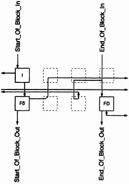
The task of performing the absolute difference is actually split between a subtracter module (Figure 6–54) and the low-order stage of the accumulator (Figure 6–55). Within the subtracter module is a bit-serial subtracter consisting of a full adder, two inverters, AND gate and unit delay. Employing a technique known as explicit subtraction (see [Denyer85] for a discussion of bit-serial operations), it takes A, B and Start_Of_Word as inputs and produces A-B. The register enabled by End_Of_Word latches the carry (borrow) at the end of each subtraction. A borrow of 0 indicates that A-B is positive and may be accumulated without modification. A borrow of 1, on the other hand, means that A-B is negative and must be negated when accumulated. The 8-unit delay aligns A-B with Sign. The low-order stage of the accumulator (top part of Figure 6–55) uses a full adder and recirculated 8-bit sums to accumulate the results of the subtracter module. If the Sign input is 0, then A-B enters the full adder unaltered and the carry input at the start of a new addition is 0. If, however, Sign is 1, then A-B is inverted and a 1 is supplied on the carry input at the start of a new addition, effectively negating A-B.
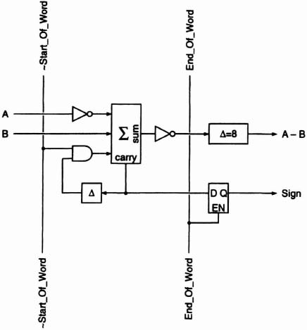
Figure 6–54. Bit-serial subtracter.
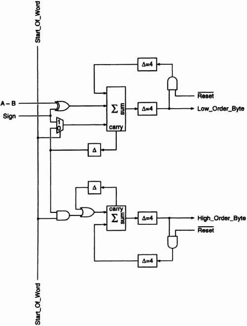
Figure 6–55. Bit-serial accumulator.
Overflow of the low-order stage of the accumulator is handled by the high-order stage (bottom part of Figure 6–55) which employs a half adder and acts as an incrementer. Whenever there is a carry out from the low-order stage at the end of addition, the value in the high-order stage is incremented by 1. (Since the high-order stage never overflows, the carry input at the start of a new operation is always 0.)
Both the low- and high-order stages make their results available and are reset at the midpoints of their 8-stage feedback paths. (The location is arbitrary and is made for the convenience of layout.)
6.8.7 Processing-element Layout
At the heart of the CLi6000 implementation of the motion-estimation algorithm is the layout for the processing-element macro. For both PE types, the CLi6000 requires just 72 cells arranged in a 2 × 36 rectangle. And because inputs and outputs on the macro’s bottom side mate perfectly with the corresponding outputs and inputs on the macro’s top side, an array of PE’s can be formed by simply plugging macros together. Because it is more complex, we provide the layout (Figures 6–56 to 6–61) for the circuit (Figure 6–53) used for all PE’s except those divisible by 16. Within each of these hard macros, there are approximately 285 equivalent gates contained in:
| 40 registers | 2 NANDs |
| 5 NAND/XORs | 2 Inverters |
| 3 Multiplexers | 1 SR Latch |
| 3 XORs | 1 AND |
| 2 Tri-state drivers |
Symbols for various cell states are explained in documentation for the CLI design environment.
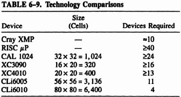
6.8.8 Technology Comparisons
At 4000 MIPS, motion estimation of a standard digital video signal easily surpasses the performance of even the most energetic uni-processors. In fact, the work reported on here began at Apple Computer where a Cray XMP could achieve only about 1/10 the performance needed for real-time motion estimation.
Figure 6–56. Overview of PE layout.
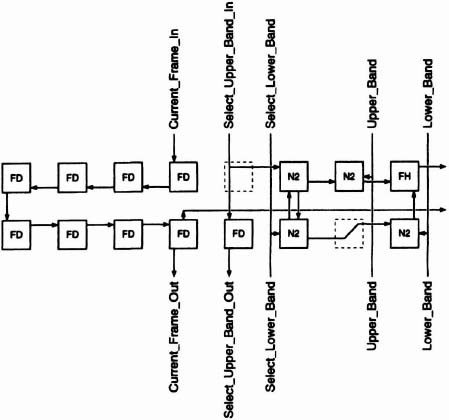
Figure 6–57. Input section.
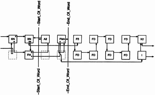
Figure 6–58. Absolute-difference section.
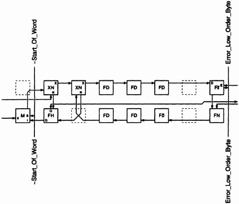
Figure 6–59. Low-order-accumulator section.
In Table 6–9, we provide comparisons of various technologies for implementing motion estimation. We make the following assumptions:
- We generously assume a performance level of 100 MIPS for the RISC microprocessor, but this is still a factor of 40 short of the 4,000 MIPS required.
- We assume that the FPGAs in the table implement the systolic array described earlier. Lower bounds for the Algotronix and Xilinx parts are based solely on register count.
- The CAL 1024 SRAM FPGA from Algotronix requires two cells to implement a register and therefore at least three rows for each processing element, which has 40 registers.
- The XC3090 and XC40 I0 SRAM FPGAs from Xilinx provide two registers in each cell (CLB), and one 20-CLB row/column contains the 40 registers needed for a processing element.
Figure 6–60. SOB & EOB section.
- The CLi6005 fits one 2 × 36 processing element in two rows. The CLi6010 available spring 1993 fits two 2 × 36 processing elements in two rows.
6.8.9 Conclusions
The CLi6000 series of SRAM-based field-programmable gate arrays provides features supporting efficient implementation of pipelined arithmetic circuits. These features are illustrated through a systolic array for motion estimation, an especially compute-intensive algorithm used in digital video compression. The CLi6000’s high register count, NAND/XOR cell states, multiplexer states, fine-grained architecture, array symmetry and high cell connectivity all work together in efficiently implementing the systolic array’s heavily pipelined, bit-serial arithmetic operations.
While only one example, this exercise suggests the suitability of the CLi6000* as a flexible alternative to hard-wired systolic arrays.
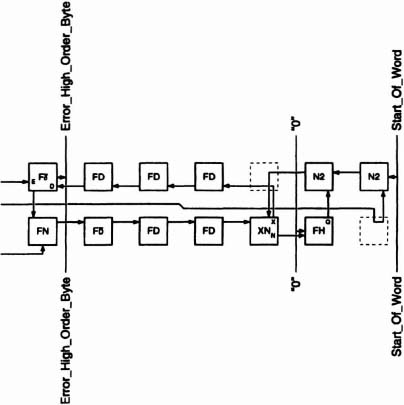
Figure 6–61. High-order-accumulator section.
PROBLEMS
Important Note: These problems explore the use of different FPGA architectures in regular structures, which would be useful in “custom computers,” for example, special-purpose processors, on a scale from a 4-bit microcontroller in one FPGA, to a RISC microprocessor implemented with a number of FPGA chips. Ideally, the exercises should be carried out with suitable CAD tools to hand, but it is still possible to sketch feasible solutions, knowing the potential as well as limitations of the individual architecture, for example, tristate capability and routing capabilities. The examples should be in two different architectures chosen from the architectures with which you have become familiar. Note that these are feasibility studies, and sketches as well as complete, detailed solutions are useful. You should estimate the size of each solution, for example, number of cells or CLBs. Also, try to give a rough estimate of speed.
- How would you implement a small pushdown stack (see figure), for example, 6 words of 4 bits? (Hint: The organization might be easier with a shift register rather than a counter.) The control signal and data locations, that is, sides, are important considerations.
- How would you implement a small scratchpad RAM (see figure), say 16 words of 4 bits? Again, assume the data and control signals are required as shown—you may change the order, but not the sides on which they appear.
(Note: It is not necessary to draw every cell in detail.)
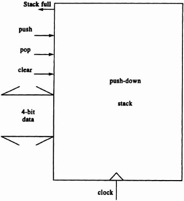
Problem 1. Pushdown stack.
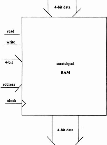
Problem 2. Scratchpad RAM.
BIBLIOGRAPHY
[Algo91] Algotronix Ltd., Configurable Array Logic User Manual, Edinburgh UK, 1991.
[Altsch90] Altschul, S. F., Gish, W., Miller, W., Myers, E. W., Lipman, D. J., “Basic Local Alignment Search Tool,” Journal of Molecular Biology, Vol. 215, pp. 403–410, 1990.
[Aptix93] Aptix Corporation, Programmable Interconnect Data Book, Aptix Corporation, San Jose, Calif., 1993.
[Arnold94] Arnold, J. M., Buell, D. A., “VHDL Programming on Splash 2,” in More FPGAs, (Moore, W., Luk, W., eds.), Abingdon EE & CS Books, U.K., 1994.
[Bertin89] Bertin, P., Roncin, D., Vuillemin, J., Introduction to Programmable Active Memories, Digital Equipment Corporation, June 1989.
[Bertin89] Bertin, P., Roncin, D., Vuillemin, J., “Introduction to Programmable Active Memories,” Systolic Array Processors, J. McCanny, J. McWhirter, and E. Swartzlander, Jr., Eds., pp. 300–309, Prentice-Hall, 1989.
[Bertin92] Bertin, P., Roncin, D., Vuillemin, J., “Programmable Active Memories: A Performance Assessment,” FPGA92, Proc. First International ACM/SIGDA Workshop on FPGA’s, Berkeley, Calif., 1992.
[Clouq87] Clouqueur, A., d’Humieres, D, “RAPI, A Cellular Automata Machine for Fluid Dynamics,” Complex Systems, Vol. 1, pp. 584–596, 1987.
[Conc92] Concurrent Logic, “CLi6000 Series Field-Programmable Gate Arrays,” Concurrent Logic, Inc., May 1992.
[D’Amour89] D’Amour, M., Sample, S., Payne, T., ASIC Emulation Cuts Design Risk, High Performance Systems, October 1989.
[Denyer85] Denyer, P., Renshaw, D. VLSI Signal Processing: A Bit-Serial Approach, Addison-Wesley, pp. 151, 196, 303, 1985.
[Furtek90] Furtek, F., Stone, G., Jones, I., “Labyrinth: A Homogeneous Computational Medium,” presented at the 1990 Custom Integrated Circuits Conference, May 1990.
[Furtek92] Furtek, F., “An FPGA Architecture for Massively Parallel Computing,” presented at the 2nd International Workshop on Field-Programmable Logic and Applications, August 1992.
[Furtek93] Furtek, F., “A Field-Programmable Gate Amy for Systolic Computing,” Research on Integrated Systems, MIT Press, Cambridge, Mass., pp. 183–200, 1993.
[Gokh91] Gokhale, M., et. al., “Building and Using a Highly Parallel Programmable Logic Array,” IEEE Computer Magazine, January 1991.
[Gray89] Gray, J. P., Kean, T. A., “Configurable Hardware: A New Paradigm for Computation.” Proc. Decennial Caltech Conference on VLSI, Pasadena, Calif., March 1989.
[Heeb92] Heeb, B., Pfister, C., “Chameleon: A Workstation of a Different Color,” Proceedings of 2nd International Workshop on Field-Programmable Logic and Applications, Vienna, Austria, September 1992.
[Hoang93] Hoang, D. T., “Searching Genetic Databases on Splash 2,” Proc. IEEE Workship on FPGAs for Custom Computing Machines, pp. 185–199, April 1993.
[Hoorn84] Hoornaert, F., Goubert, J., Desmedt, Y., “Efficient Hardware Implementation of the DES,” Advances in Cryptology, Proc. Crypto 84, Springer-Verlag, 1984.
[Hoorn88] Verbauwhede, I., Hoornaert, F., Vandewalle, J., “Security and Performance Optimisation of a new DES Data Encryption Chip,” IEEE Journal of Solid-State Circuits, Vol. 23, pp. 647–656, June 1988.
[Kean89] Kean, T. A., “Configurable Logic: A Dynamically Programmable Cellular Architecture and Its VLSI Implementation,” Ph.D. Thesis CST-62-89, University of Edinburgh, Dept. Computer Science, 1989.
[Konh85] Konheim, A. G., Cryptography, a Primer, Wiley, 1985.
[Lipton85] Lipton, R. J., Lopresti, D. P., “A Systolic Array for Rapid String Comparison,” in 1985 Chapel Hill Conference on VLSI, (Fuchs, H., Ed.), Computer Science Press, pp. 363–376, 1985.
[Lyon76] Lyon, R., ‘Two’s Complement Pipeline Multipliers,” IEEE Transactions on Communications, pp. 418–425, April 1976.
[Masek83] Masek, W. J., Patterson, M. S., “How to Compute String-Edit Distances Quickly,” in Time Warps, Siring Edits, and Macromolecules: the Theory and Practice of Sequence Comparison, (Sankoff, D., Kruskal, K., eds.), pp. 337–349, Addison-Wesley, 1983.
[NBS77] National Bureau of Standards, Data Encryption Standard, Fed. Inf. Process. Stand. Publ. 46, January 1977.
[NBS80] National Bureau of Standards, DES Modes of Operation, Fed. Inf. Process. Stand. Publ. 81, December 1980.
[Oldfield91] Oldfield, J. V., Kappler, C. J., “Implementing Self-Timed Systems: Comparison of a Configurable Logic Array with a Full-Custom VLSI Circuit,” FPGA’s: Proceedings of the International Workshop on Field Programmable Logic and Applications, (Moore, W., Luk, W., eds.) Abingdon EE & CS Press, 1991.
[Prest84] Preston, K., Duff, M., Modern Cellular Automata, Plenum, New York, 1984.
[Shimom87] Shimomura, T., Doolen, G. D., Hasslacher, B., Fu, C., “Calculations Using Lattice Gas Techniques,” Los Alamos Science (Special Issue), 1987.
[Stormon90] Stormon, C., Rapid Genome Analysis on a Workstation with an Associative Coprocessor, Phase I Final Report for the U.S. Department of Energy, Coherent Research Inc., Syracuse, N.Y., April 1990.
[Suther89] Sutherland, I. E., “Micropipelines,” Communications of the ACM, Vol. 32, No. 6, pp. 720–738, June 1989.
[Tanenb81] Tanenbaum, A. S., Computer Networks, Prentice-Hall International, 1981.
[Thomae91] Thomae, D. A., Petersen, T. A., Van den Bout, D. E., ‘The Anyboard Rapid Prototyping Environment,” Advanced Research in VLSI 1991, University of California at Santa Cruz, Santa Cruz, pp. 356–370, 1991.
[Toffoli87] Toffoli, T., Margolus, N., Cellular Automata Machines, MIT Press, 1987.
[Tse92] Tse, K. W., Yuk, T. I., Chan, S. S., “Implementation of Data Encryption Standard Algorithm with FPGAs,” Proceedings of 2nd International Workshop on Field-Programmable Logic and Applications, Vienna, Austria, September 1992.
[Wayner88] Wayner, P., “Modelling Chaos,” Byte, pp. 253–258, May 1988.
[Wolfram86] Wolfram, S., Theory and Applications of Cellular Automata, World Scientific, Singapore, 1986.
Section 6.4 contains contributions by Christopher Kappler and originally appeared in “FPGAs,” (Moore, W., Luk, W.) Abington EE & CS Books, 1991.
Section 6.5 was contributed by Christopher J. Kappler, Kang Shen, John Oldfield, and Charles Stormon, and originally appeared in “More FPGAs,” (Moore, W., Luk, W.) Abingdon EE & CS Books, 1994.
*The assistance of Dzung T. Hoang and Jeffrey M. Arnold is gratefully acknowledged. The work was supported by the New York State Center for Computer Applications and Software Engineering at Syracuse University.
Section 6.8 was contributed by Frederick Furtek and originally appeared in Research on Integrated Circuits: Proceedings of the 1993 Symposium, Gaetano Boniello and Carl Eberling, Eds. © 1993 Massachusetts Institute of Technology.
*See [Conc92] for a more complete description of the CLi6000 architecture.
† The accumulator has high- and low-order bytes because although the maximum difference between two pixels is 11111111 (255), the maximum accumulated error between two blocks is 1111111100000000 (256 × 255 = 65,280).
‡The unit delay just before the A input of the absolute-difference module is only for pipelining. Small delays on various array inputs, including CF, may have to be inserted to insure correct alignment.
§We are ignoring the latency in the absolute-difference module and the accumulator. Once these values are known, both the SOB and EOB signals will have to be delayed prior to PE 0 by an appropriate amount to compensate.
¶Because the accumulator is bit serial, the high-order byte is accumulated one word (8 clock periods) after the low-order byte.