
8.4 CONFIGURABLE LOGIC ARRAYS AND PROTOTYPING BOARDS
In Chapter 6, we saw how regular arrays of FPGAs could provide a high-performance custom-computing environment. The Algotronix CHS2×4 board took advantage of an unusual feature of the CAL architecture, that is, chips can be cascaded in any of the four principal directions, without much concern to effects at chip boundaries.
8.4.1 The XESS RIPP Board
The RIPP is a PC-based reconfigurable system containing up to eight Altera FLEX 8000 FPGAs or I-CUBE FPIDs on a single card. The FPGAs and FPIDs can be used interchangeably, thus allowing the user to trade off logic and I/O resources for a given application. The RIPP also has four 512K × 8 RAMs for data storage and another FLEX FPGA, which manages the interfaces between the RIPP, the PC, and the external world.
Fundamental Components The Altera FLEX81188 packs 12,000 logic gates into a 17 × 17 pin-grid array (PGA) package. So if all eight sockets are loaded with FPGAs, the RIPP can support applications needing up to ≈ 100,000 gates.
The IQ160 FPID described in more detail earlier in this chapter has a 160 × 160 crossbar architecture that can realize any interconnection pattern without the need for complex routing. Since the IQ160 and the FLEX81188 have roughly the same amount of I/O (160 pins versus 184 pins), a single socket can support either device via the use of an adapter.
RIPP Internal Architecture The bussing arrangement that interconnects the eight RIPP sockets is shown in Figure 8–27. The underlying interconnection pattern is a bipartite graph with sockets {1,3,6,8} in one partition and sockets {2,4,5,7} in the other partition. Each socket has a separate 32- or 46- bit local bus going to every socket in the other partition, but sockets within the same partition not directly connected. If communication within a partition is necessary, it can be passed through one of the FPGAs or FPIDs in the other partition. Each FPGA or FPID can also send and receive data over a 36-bit global bus that connects to all eight FPGA/FPID sockets.
A RAM resides between each of the following pairs of sockets: {1,2}, {3,4}, {5,6}, {7,8}. The RAM and the pair of FPGA/FPIDs are connected by a 46-bit local bus. All 46 wires of this bus can be used to transfer data between the FPGA/FPIDs, or 30 of the bus lines can be used to access the 512K × 8 static RAM (the other 16 wires are still usable for FPGA/FPID data transfers). Either or both FPGA and FPIDs can generate the address and control signals, and either or both FPGA and FPIDs can use the RAM data. With this interconnection scheme, the RAMs could also be replaced by other types of chips that the FPGA and FPIDs might use for special-purpose applications.
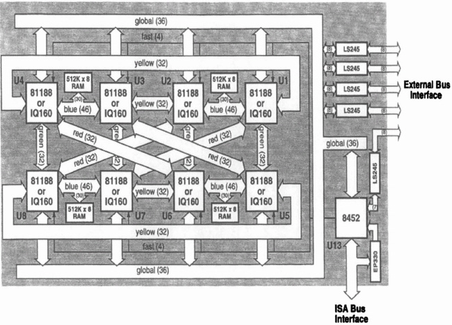
Figure 8–27. RIPP bussing and interfaces.
The IQ160 FPID has fewer I/O pins than the Altera FLEX81188, so when an FPID is placed in one of the sockets it only connects to 18 lines of the 36-bit global bus. This is a small loss, since the global bus already interconnects all the FPGAs, and rerouting these connections using an IQ160 has few benefits. But, by connecting the IQ160 to the full 46-bit local bus, it becomes possible for a FPGA to access RAMs in other elements by routing address and data signals through the IQ160. This adds another level of flexibility to the RIPP.
RIPP External Interfaces There are two interfaces to the RIPP: one to the outside world and one to the host PC. An Altera FLEX8452 FPGA controls the passage of data through each of these interfaces.
The interface to the outside world goes through an 80-pin nanoconnector. Forty of these signal lines are grounded and the other 40 lines are organized into five individually controlled banks of eight bits each. Four of these bytewide signal banks connect to the global bus and can be either inputs or outputs. The remaining byte-wide bank is connected to the FLEX8452 and is used to manage the transfer of data over the external interface.
The RIPP resides in the I/O address space of the PC host. The FLEX8452 FPGA can be programmed to support polled, interrupt, or DMA types of operations over the Industry Standard Architecture (ISA) bus of the host PC.
Reconfiguring the RIPP Loading an application into the RIPP through the ISA bus requires the following main phases:
1. Configuring the FLEX8452 with the standard downloading interface
2. Configuring the FLEX81188s
3. Configuring the IQ160s
4. Reconfiguring the FLEX8452 with the custom interface required by the application (optional)
Because each application may need a specialized interface to the host PC, the FLEX8452 has no fixed configuration EPROM. Instead, a small Altera EP330 PLD on the RIPP serves as a “boot loader” that manages the configuration of the FLEX8452 over the ISA bus. By writing to addresses in the range 0x31C-0x3IF, the PC can program the FLEX8452 to act as a downloading interface for the FLEX81188s and IQ160s on the rest of the RIPP. Once configured, the FLEX8452 accepts configuration data from the ISA bus and uses it to configure any FLEX81188 FPGAs on the RIPP via the global bus. Next, the FLEX8452 takes configuration data for any IQ160 FPIDs on the RIPP and programs them through their JTAG interface. Once the main array of FPGA/FPIDs is configured, the FLEX8452 can be reconfigured to support any type of specialized interface needed by the application.
RIPP Applications For applications with very regular interconnection structures, such as signal processing or neural networks, an RIPP loaded only with FPGAs is often suitable. The RIPP bus arrangement supports a simple data pipeline, mesh, or torus, among others. The 36-bit global bus provides sufficient bandwidth for transmitting global data and/or control signals to the processing elements residing in the FPGAs.
Many applications, such as an emulated microprocessor, have less regular communication paths. A microprocessor emulator can be built by assigning the microsequencer, arithmetic logic unit (ALU), register set, and memory manager to individual FPGAs and interconnecting them through FPIDs loaded in the remaining sockets. Because of the interconnection topology, each FPID is connected to each FPGA through a wide 32- or 46-bit bus. This provides ample control lines from the microsequencer to each of the other sections. The other sections are equally well connected so that data can be exchanged between the register set and the ALU, for example. In addition, the RAMs can be used to hold microprograms, windowed register sets, and to emulate system memory.
Conclusion The RIPP is an attempt to bring reconfigurable systems to a larger audience. It uses a commonly available host computer, possesses a bus structure applicable to many applications, allows trade-offs to be made between logic density and signal routing, and has a very reconfigurable I/O interface.