
6.3 DES ENCRYPTION
In 1977 the United States National Bureau of Standards (NBS) promulgated a new standard for encryption of unclassified data [NBS77] based on a proposal by IBM, the Design Encryption Standard (DES). Since then, this algorithm has become the de facto standard for data encryption worldwide. The algorithm is very suitable for implementation in hardware and several commercial products are available. In this section, we first outline the DES algorithm and secondly develop an implementation. DES provides an excellent example of an algorithm that can be speeded up greatly by bit-level hardware implementation. In this section, we develop a CAL implementation of DES: a more detailed presentation of this work appeared in [Kean89].
DES is a substitution cipher on 64-bit binary vectors based on a 56-bit key. The strength of DES lies in the complexity of the substitution. Two good introductions to DES are [Tanenb81], and for a more in-depth analysis [Konh85].
6.3.1 The DES Process
The DES algorithm is illustrated in Figure 6–4. All the f-boxes are identical, and it is obvious that a major design decision is whether to have one reusable f-box, or 16 separate ones to allow pipelining. We will consider the major components in the block diagram individually. We will try to give an idea of the size of the wiring channels (unfortunately channel density cannot be quoted because it depends on the ordering and spacing of the ports, which is implementation-dependent) and we will give the number of product terms in a minimized PLA implementation (determine using ESPRESSO) for the logic blocks.
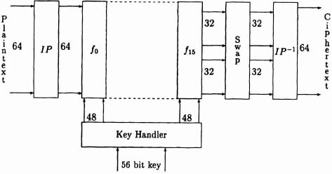
Figure 6–4. DES block diagram.
Permutations IP and IP−1 The first step in the DES algorithm is to apply an initial permutation IP to the plaintext. The permutation is applied in reverse IP−1 as the final step. These permutations involve simple wire swapping and could be implemented using the channel router, but the resulting channel would be wide. The permutations are highly structured and more cost effective implementations than straightforward wire swapping can be found.
Design of the ![]() -Box The heart of the DES process is the f-box, which performs the function π :(L, R) → (R, L ⊕ T(R)), where L and R represent the left and right 32 bits of the 64-bit input. The transformation T is composed of an expansion (bit copying) to 48 bits modulo 2 addition with a key, substitution (in which each group of 6 bits is taken as representing a binary number, which is then substituted for another 4-bit binary number using a lookup table, bringing the size back to 32 bits) and a 32-bit permutation (wire swapping).
-Box The heart of the DES process is the f-box, which performs the function π :(L, R) → (R, L ⊕ T(R)), where L and R represent the left and right 32 bits of the 64-bit input. The transformation T is composed of an expansion (bit copying) to 48 bits modulo 2 addition with a key, substitution (in which each group of 6 bits is taken as representing a binary number, which is then substituted for another 4-bit binary number using a lookup table, bringing the size back to 32 bits) and a 32-bit permutation (wire swapping).
The major components in the DES f-box are illustrated in Figure 6–5. The important point to note is that the width of any hardware implementation is fixed by the number of bits to be operated on. We must concentrate on reducing the length of the unit. We will now consider the components of the f-box in order, left to right.
- Expansion. This step involves expanding groups of four bits in the data to six bits by copying the outer two bits as shown in Table 6-2. This step fixes the height of the implementation as at least 48 cells.
- XOR with key. This is the critical operation in the whole cipher since this is the only point where the output ciphertext is modified by the key. A different 48-bit key derived from the user-supplied 56-bit key is used in each f-box.
Figure 6–5. DES f-box block diagram.
Before After x0, x1, x2, x3 x31, x0, x1, x2, x3, x4 x4, x5, x6, x7 x3, x4, x5, x6, x7, x8 x8, x9, x10, x11 x7, x8, x9, x10, x11, x12 x12, x13, x14, x15 x11, x12, x13, x14, x15, x16 x16, x17, x18, x19 x15, x16, x17, x18, x19, x20 x20, x21, x22, x23 x19, x20, x21, x22, x23, x24 x24, x25, x26, x27 x23, x24, x25, x26, x27, x28 x28, x29, x30, x31 x27, x28, x29, x30, x31, x0 - S-Box. The S-box or substitution box has 4 outputs and takes 6 inputs, 4 “data” and 2 “control.” The control inputs select one of four 1-to-1 substitution functions over 4-bit binary integers. There are eight separate S-boxes, each of which uses different functions. These units are most naturally implemented as blocks of combinational logic. Running the functions through ESPRESSO produced very little minimization; all 8 S-boxes required more than 50 product terms. This is presumably because the cryptographic properties of DES require an irregular function, whereas logic minimization relies on finding regularities.
- P-Box. The P-Box or permutation box does a simple wire-swapping operation on its inputs. The layout can be realized with a channel-router, given a reasonable area.
- XOR and Swap. The swap is necessary because without it only the right half of the plaintext would interact with the key. This would imply that 32 bits of the ciphertext would be identical to 32 bits in the plaintext (which 32 bits in ciphertext and plaintext would depend on the initial and final permutations). The XOR is also crucial to the complexity of the cipher because without it there would be two groups of 32 bits in the ciphertext, each of which depended only on a group of 32 bits in the plaintext. Instead of being a 64-bit, 16-stage cipher, it would be two separate 32-bit, 8-stage ciphers and hence much easier to crack.

Final Swap The final swap has the effect of canceling out the swap in the final f-box. This cancellation is done to keep the cipher symmetrical so that decryption can be done by reencrypting with the same key; thus only one DES unit is required (not two, one for encryption and one for decryption).
Design of the Key Handler This logic controls the key that is applied to the f-box at each stage of the DES operation. This logic is determined by the key-schedule. The design of the key-handling unit is shown in Figure 6–6. We describe the major components in turn.

Figure 6–6. DES key handler.
- PC1. The PC1 unit applies an initial permutation to the bits of the key. This unit is 56 bits wide. It can be implemented using a channel router, but the channel is fairly wide and better implementations based on the structure of the permutation are possible.
- Shifters. After the initial permutation the key is broken up into two 28-bit segments C and D which do not come into contact with each other again. At each stage in the cipher the C and D keys are shifted circularly a number of times, determined by the controller according to the key schedule.
- PC2. The PC2 unit takes the C and D input keys and does a selection and permutation operation on them, selecting 48 bits from the 56-bit key. The top 24 bits of the result all come from C and the bottom 24 bits all come from D, so it is possible to view PC2 as being two separate 28 to 24 bit units. The resulting 48-bit number is used as the key in the f-box. Again this unit can be implemented using a channel router, and in this case the channel is reasonably small.
- Controller. The controller generates either one or two clock pulses for the shift registers at each stage of the cipher according to whether one or two key shifts are specified in the key schedule.
6.3.2 Implementation of DES
Floorplan When we consider the amount of logic required to implement an f-box, it becomes obvious that we cannot hope to have 16 of them in a reasonable sized array. Instead, we must use the same box for every stage of the cipher. We wish to avoid bringing the key in from the bottom because at least 48 cells will be required to input a 48-bit vector: if it is brought in from the side, then no extra cost is incurred because the unit must be at least 48 cells high anyway. We also note that IP and IP–1 can be implemented in the same wiring area. This suggests the floorplan shown in Figure 6–7.

Figure 6–7. DES floorplan.
Layout of ![]() -Box When we examine Figure 6–5 it appears that large wiring areas will be required for the L and R 32-bit words. It is also apparent that all the signals go from left to right: this would imply a large waste of cell resources since the basic cell can route right to left as well. After a little thought, it becomes clear that a much better layout of the f-box is possible (Figure 6–8). By using registers at the right-hand side we have avoided wasting large areas transporting L and R through the unit. By interleaving L and R we have made it extremely easy to XOR adjacent bits and swap over prior to the next stage. We are making use of the cell’s ability to route R right to left to bring it to the left-hand side for the initial expansion and XOR with the key. We now consider the design of the major f-box components in turn.
-Box When we examine Figure 6–5 it appears that large wiring areas will be required for the L and R 32-bit words. It is also apparent that all the signals go from left to right: this would imply a large waste of cell resources since the basic cell can route right to left as well. After a little thought, it becomes clear that a much better layout of the f-box is possible (Figure 6–8). By using registers at the right-hand side we have avoided wasting large areas transporting L and R through the unit. By interleaving L and R we have made it extremely easy to XOR adjacent bits and swap over prior to the next stage. We are making use of the cell’s ability to route R right to left to bring it to the left-hand side for the initial expansion and XOR with the key. We now consider the design of the major f-box components in turn.
- S-Box. Westart with the S-box because it is the most complex component and will constrain the rest of the design. In order to make use of the logic synthesizer described in Chapter 4, we have to adopt an AND plane/OR plane type layout for this unit with six input signals and four output signals. This means that the design will be nine or ten cells wide, depending on the logic synthesis method used. We can see from the floorplan that as well as performing the logic function, the S-box unit must route four bits of the R vector right to left: this is easily done using the right-to-left connections in the OR-plane. All the S-boxes will be expanded to be the same width as the one with the largest number of product terms.
The S-boxes were implemented using the CAL ROM generator and required 32 product terms. Although the logic block is only nine cells wide, we choose to use an extra line of cells between each S-box unit, making its effective width 10 cells and fixing the height of the f-box at 80 cells. There are two advantages to this: first, by increasing the height of the wiring channels we simplify the routing problem, allowing a solution using fewer tracks; second, the extra width simplifies the design of the other f-box components.
Figure 6–8. F-box floorplan.
The S-box outputs are generated in the order in which they appear on the opposite side of the P-box wiring channel rather than the “numerical” order of the standard. This reduces the number of tracks required to implement the P-box. Note that the right-to-left connection of R shown on the diagram is accomplished by overlaying a routing symbol on the automatically generated S-box design: this is possible because the right-to-left connections are not used by the ROM.
- Expansion and Key XOR. It turns out to be easier at the cellular level to implement both these functions within the same subunit. Note that there are in fact three slightly different designs for the first, last, and intermediate expansion units because there is a (x0, x31) wraparound connection. The 80-cell path for this wraparound connection is the limiting factor for pipelining this design. All but the first two columns of cells in the expansion unit are overlaid on the S-box, so its effective width is only two cells: note the extra routing to bring the last bit of K ⊕ R to all the OR plane columns of the ROM.
- P-Box. The P-box is a large wiring channel that runs the whole length of the f-box. As well as implementing the wire swapping, it also realigns the ports ready for the next stage. The R vector can travel across the top of the wiring channel very easily since no right-to-left connections will be used: there is no need to inform the channel router about these signals.
- L/R Registers XOR and Swap. The L and R registers are implemented as master-slave flip-flops to allow a new value to be loaded while keeping the previous value stable. The registers are broken down into 4-bit units which occupy 10 cells (pitch matched to an S-box). Within these units the bits are interleaved: swapping is implemented simply by a transfer between adjacent registers.

The layout of the whole unit is given in Figure 6–9. Note how the individual components fit together and that the signal flow scheme allows a very high utilization of cell resources.
Layout of Key Handler The layout of the key handler can follow the block diagram exactly. We will consider the implementation of the major subcomponents in turn.
- PC-1. This routing converts eight 8-bit bytes into a 56-bit number by throwing away the most significant bit of each byte and doing some simple scrambling of the remaining bits. It is questionable whether it is worth the overhead of hardware implementation, since it will only be used when the key is changed, and this is a relatively rare event. Fortunately, the permutation is structured in such a way that it can be implemented using shift registers rather than a large wiring channel [Hoorn84]. The shift register technique is explained in more detail for the IP channel discussed later: its application to this channel is slightly less straightforward.
- Shifters. These are implemented as clocked master-slave registers with a feedback path. The shifters are pitch matched to the controller in width and to the wiring channels in height. The number of clock pulses determines the number of shifts. The layout is given in Figure 6–10.
- Controller. This unit can be implemented simply as a finite state machine using the logic synthesizer. It must generate either one or two clock pulses for the shifters on each f-box cycle: to do this it is clocked twice at the start of each f-box cycle and cycles around a 32-state sequence. The reset signal clears the state machine ready for the first cycle and is routed to the shift registers to load the next key through PC-1. When reset is low the registers are configured as two 28-bit circular shifters. In this case Papakonstantinou’s algorithm [Kean89] provides a slightly better solution that the ROM generator. A small amount of manual routing is necessary for the feedback terms: the generator could easily be extended to do this automatically. Note that the layout (Figure 6–11) could be optimized by using unused multiplexers within the logic array to provide the feedback connections.
Figure 6–9. F-box layout.
Figure 6–10. Shifter layout.
- PC-2. This unit is implemented using the channel router: it performs a permutation and selection operation on the shifted 56-bit key to generate a 48-bit key for the f-box. Since only 48 bits are used some of the ports on the left of this wiring channel are unconnected.


The layout of the whole unit is given in Figure 6–12.
IP and IP–1 The initial permutation is given in Table 6-3. A straightforward implementation of this large wiring area would require at least 37 cells. The size of this requirement has to do with both the permutation itself and the fact that we are implementing both IP and IP–1 in the same channel. This means that there are 64 input and 64 output ports on both sides of an 80-cell channel heavily constraining the channel routing (there are very few “free” columns that the router could use to reorder nets). This channel is a problem for silicon implementations of DES as well, and we can borrow a technique from [Hoorn84], [Hoorn88] to implement it in a reasonable width. The technique relies on regularities in the IP permutation and replaces the large channel with a small one and some shift registers: it has the side effect of reducing the data rate, but this is not a problem since the speed of the implementation is constrained by the f-box circuits, which are used sixteen times for every input through IP. The design is shown in Figure 6–13 and the layout in Figure 6–14.
6.3.3 Pipelining
The design of DES encryptor just described would be unnecessarily slow because of the accumulated delays through the f-box. It was decided, therefore, to separate the f-box into four pipelined stages to increase throughput. Note that the delays within the key controller and the IP unit are relatively unimportant because the computation within the f-box is much more complex and is repeated sixteen times for every data input, and keys are changed relatively infrequently. Any reasonable design of these units will be able to keep the f-box supplied with data and keys.

Figure 6–11. Key control state-machine layout.

Figure 6–12. Key control unit layout.

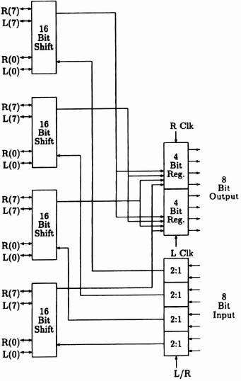
Figure 6–13. IP design.

Figure 6–14. IP unit layout.
It was decided to aim for a throughput of 500,000 encryptions per second with a constant key. To achieve this rate, one 64-bit ciphertext word must be calculated every 2 μs. Since the f-box unit is used sixteen times for each ciphering operation, partially ciphered data must leave the f-box every 125 ns. Table 6-4 shows the approximate delays through the major f-box components (we take routing delay through one cell as 2.7 ns and calculation and output routing delay as 10 ns—these figures are for 256-cell CAL chips designed in 1987, the CAL 1024 devices are faster). We can see that some of these components must be broken up into several pipeline stages to meet the performance objective. The last column of the table shows the number of stages required. Within the CL-ROM we choose to place pipeline registers between the AND and OR planes as well as horizontally across the array. This decouples the AND plane calculation time, which is quite high since there are six inputs. With pipelining between the planes as well as three stages across the array (two with 11 product terms and one with 10) we have a stage delay of (m – l)r + 11c = 3 × 2.7 + 11 × 10 = 118.1 ns. The ability to pipeline these large combinational logic units is a partial compensation for the loss in speed caused by using large numbers of 2-input gates rather than a single high fan-in gate. Pipelining within wiring channels is easy to provide using the function units of the cells within the channel.
With the suggested pipelining, the only stage that is close to the 125-ns limit is in the KEYXOR unit—if this proved to be a problem, a slightly more complex routing arrangement could split the 80-cell top-to-bottom wraparound connection among several of the right-to-left routing stages—extra pipeline stages would not be required. The total pipeline length is 10 stages. Extra registers must be provided at the right side of the f-box unit to store the ‘L’ vectors corresponding to the ten ‘R’ vectors at the various pipeline stages within the f-box. The pipeline registers themselves are fairly small, requiring only two cells for each master-slave register. They are clocked using the G1 and G2 global signals since propagation delay on the pipeline clock is an important consideration.

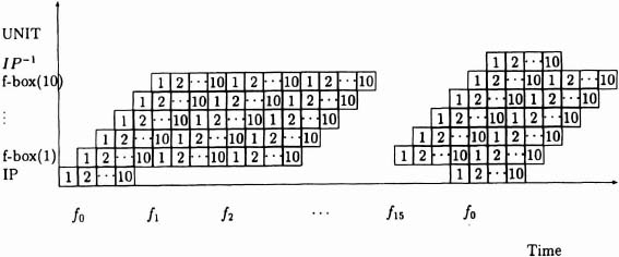
Figure 6–15. Pipelining scheme.
The time-line for the pipelining scheme is given as Figure 6–15. The delay through the f-box is 16 ∗ (10 ∗ 125 ns) = 20 μs. It seems natural to pipeline the input and output phases through IP, with this giving a total delay through the encryptor of 60 μs. In applications where large amounts of data have to be encrypted the throughput is of paramount importance, so this is a reasonable design. We could, however, reduce the delay to around 25 μs by removing the extra IP pipelining at a small cost in throughput.
6.3.4 Performance
The performance of DES implementations can be measured in two ways: the number of encryptions per second with the same key and different data, and the number of encryptions per second with a different key and the same data. The second metric corresponds to ‘key-trial’ in an attempt to break the cipher, the first to normal use of the cipher. The present design is optimized for normal use, so we will concentrate on this problem. Table 6-5 shows figures for some DES implementations: the figures for SUN workstations are using the UNIX crypt function in the C library. This implementation is not particularly efficient and it is likely that the times could be significantly improved by recoding in assembly language and taking advantage of space-time trade-offs by using large data arrays to compute S-box functions. The time for a single encryption is given, as well as the number of encryptions per second to show the effect of pipelining. The transputer array figure is a notional one assuming 1000 transputers and that each transputer has a good DES program, allowing encryption ten times faster than a SUN 3/260: it is intended to illustrate the limitations of conventional parallel computers in this application. The time for the custom chip is taken from [Hoorn88]. This claimed to be the fastest DES chip available with a throughput of 32M bits/sec (or 500,000 64 bit words/sec). Note that this chip has extra control logic to handle the more complex modes of DES defined in [NBS80] and also provides several registers for secure storage of keys on the chip. The CAL design makes use of several optimizations developed by the group that designed this chip. Although the CAL appears to be as fast, it should be pointed out that 3-μm processing technology was used in the custom chip, which would be expected to be slower than the 2-μm technology on the CAL, and the CAL figures are based on circuit simulations rather than measurements on fabricated chips.

The CAL implementation of DES (including pipeline registers) requires an array of cells 88 cells high by 90 cells wide (27 for the key controller, 60 for the f-box, and 13 for IP). This could be provided using a 6-by-6 array of 16 × 16 CAL chips or a 3-by-3 array of 32 × 32 CAL1024 chips. The entire DES encryptor would fit on a single printed circuit board even with low-density 16 × 16 chips.