
3.3 STRUCTURED PROGRAMMABLE ARRAY LOGIC
Before examining structured PALs, we will look at a simpler concept, the programmable read-only memory (PROM) as applied to two-level programmable logic. The idea is simple: a lookup table with n inputs, m outputs, and 2n rows. The PROM is attractive because:
- Given the number of inputs and outputs, one can specify a given device before determining the actual logic function to be implemented. This is a powerful capability since it allows the PCB design to be started before the logic design is completed. It also allows for PROM design upgrades after the PCB design is finalized.
- The delay through the programmable device is constant and independent of the logic function implemented: again this is a powerful property, allowing (he separation of timing verification from logic design.
- The function of the device can be specified at a high level as a series of logic equations or as a truth table, allowing rapid design.
There are two major drawbacks with the PROM architecture that have prevented it from becoming dominant in the marketplace:
- Silicon area, and hence cost, and sometimes more importantly, package and board area, is determined by the number of product terms. There are 2n product terms in an n input PROM.
- Delay through a PROM is proportional to the number of product terms, and hence scales badly as the number of inputs increases.
For these reasons PROMs are only suited for those functions where it is necessary to completely decode the input signals: a good example might be a lookup table for converting character codes from one set to another.
In full-custom design, programmable logic arrays (PLAs), for which both AND and OR planes are programmable, are the dominant method of implementing medium-to-large-size arbitrary logic functions. The programmable equivalent of these devices have, however, failed to penetrate the programmable logic market to a significant extent. This is because the extra layer of programmability increases delay, while programmable PLAs no longer provide the property of PROMs that all functions of n variables can be implemented. Instead a fixed smaller number of product terms must be chosen a priori by the device designer, with the consequence that devices can no longer be selected solely on the basis of the number of input and output variables. Similarly any change to the function to be implemented may result in it no longer fitting the chosen device.
By far the most common architecture in the programmable logic market today is the PAL, where the AND plane is programmable but the OR plane is fixed, with a small number of product terms contributing to each output variable. Figure 3-7 shows a simple commercial device, the 16L8, so-called because there are 16 inputs to the AND plane and 8 outputs from the OR plane. Some of the device pins are dedicated inputs and some are programmable input outputs (I/O2..I/O7). OR plane outputs on I/O2..I/O7 can also feed back into the AND array.
This PAL architecture is predicated on the observation that a large class of real designs require relatively few product terms per output. The key advantage of this architecture is that speed can be high because there are no longer wide wired ORs in the OR plane. One important disadvantage when compared to PLAs is that product terms are now dedicated to a particular output pin, and so multiple copies of particular product terms may be required. A design can fail because a particular output does not have enough product terms, despite the fact that the total number of product terms required is smaller than those provided. It can be painful when a proposed change to logic within a PAL on an existing PCB requires more product terms on a particular output than the chosen device supports!
One obvious question from the preceding discussion is why are PALs not the solution to all programmable logic needs? Why not just go out and buy a 50L50 device to do any reasonable design with up to 50 inputs and 50 outputs? There are at least two problems:
- Delay is also influenced by the AND plane, both in terms of the length of wires required to reach individual product terms and the width of each product-term-wired AND area (twice the number of inputs because both true and complement forms of input variables are required). Thus in equivalent technology, a 50-input PAL might be three times as slow as a 16-input PAL: so if your particular application could be implemented in a small number of 16L8s or a single 50L50, you might well choose the 16L8s.
- If one implements a large logic function using several small PALs, one can choose each PAL from a catalog providing a range of options in characteristics such as number of inputs, number of outputs, and number of product terms per pin. Thus, it may be appropriate to choose a PAL with eight product terms per output for some output variables and one with two product terms per output (but more outputs) for others. One can also use the routing flexibility of the PCB to route different input variables to different PALs and to use outputs from one PAL as inputs to another. A straightforward extension of the PAL architecture in which every output had the same number of product terms, all input variables were fed to all output product terms, and all outputs had feedback terms, would be much less efficient in terms of the total number of fuses required.
Structured PAL designs address these efficiency problems by simply extending the basic PAL architecture while preserving its speed and ease of use. The key commercial examples of structured PALs are the Altera devices. We now briefly consider the Altera EP1810: this device has been chosen because it illustrates the main components of the structured PAL architecture, while still being simple enough to serve as an introductory example. State-of-the-art structured PALs offer more of the same.

Figure 3-7. PAL 16L8 logic diagram. (Notes: (1) All unprogrammed or virgin AND gate locations are pulled to logic “1.” (2) Programmable connections.) Copyright © Advanced Micro Devices. Inc. 1993. Reprinted with permission of copyright owner. All rights reserved.
3.3.1 The Altera EP1810
Figure 3–8 shows the basic architecture of the device. There are two varieties of macrocell (corresponding to OR plane outputs in the 16L8); Figure 3–9 shows a “local” macrocell; and Figure 3–10 a “global” macrocell. Note the architecture is very similar to that of the classic 16L8 device, except that there are now two classes of product terms: local and global. This difference is motivated by the realization that many nets in most designs do not have to be routed to every gate! For roughly the same silicon area there are four times as many loc al nets as possible global nets, so larger designs can be implemented. The price for this is that one has introduced a simple placement and routing problem. One has to select where to place a particular piece of logic on the device with regard to its connectivity and one can no longer guarantee that a design will fit on the device, given the number of output macrocells and input variables required.

Figure 3–8. EP1810 block diagram. (Reprinted with permission from Altera Corporation)

Figure 3-9. EP1810 local macrocell. (Reprinted with permission from Altera Corporation)
The box labeled IO Architecture Control provides additional flexibility in the use of the output pin: for example, conditional inversion, along with input and output latching. There is considerable flexibility in the choice of clocking scheme applied to these registers. The ability to conditionally invert the output can allow functions to be implemented using fewer product terms. For example, the function f = X0 * X1 * X2 * X3 requires a single product term, while the function ![]() requires four. This facility can make the difference between a function fitting in a single macrocell and overflowing.
requires four. This facility can make the difference between a function fitting in a single macrocell and overflowing.
Although in this device all macrocells have the same number of dedicated product terms, in some structured PALs different macrocells have different numbers of product terms. This can result in more efficient mapping of user designs, avoiding unused product terms in some macrocells, and the need to cascade macrocells to build more complex functions in other places. Another capability of some devices is that some product terms can be shared between adjacent macrocells programmably connected to the OR planes of both, so that they can be assigned to one or the other, depending on the demands of the design.
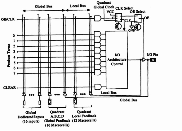
Figure 3-10. EP1810 global macrocell. (Reprinted with permission from Altera Corporation)
As can easily be surmised from the preceding description, use of complex PLDs is dependent on “fitter” software, which attempts to match the requirements of the user's design with the resources supplied by the PLD. As well as logic minimization, the software must match the number of product terms and input variables required by an output with those available from different macrocells. Some degree of intelligence is required by such algorithms. An unavoidable side effect of this approach is that a small change in the user's input specification could result in a design no longer fitting a particular device or requiring pinout changes resulting from changes in macrocell assignments. Either of these outcomes is undesirable if PCB design has been completed.