
8.5 CAD SUPPORT
We have seen that the designer’s requirements can range from virtually automatic design, in which the user simply desires that the logic be packed into a given FPGA chip, and to run at the speed desired for the application, to more sophisticated ones, in which the user needs to control the detailed organization of a cell in, say, a systolic array. CAD support can be effective at many stages, including minimization steps, which are sensible for any implementation, that is, they are technology-independent.
8.5.1 NeoCAD Foundry
NeoCAD, Inc., based in Boulder, Colorado, has a unique strategy toward delivering an open FPGA design environment, which it refers to as FPGA Foundry. As an independent FPGA CAD tool supplier, NeoCAD provides a single set of high-performance tools supporting the many different architectures offered by a growing number of FPGA vendors. This focused strategy enables technology-transparent design, allowing the engineer to optimize cost and performance as the design progresses. Development tools include the Timing Wizard for timing and frequency-driven design, the Prism logic partitioning system, the HYDRA client/server place-and-route engine, and CAE tool integration.
The FPGA design process using FPGA Foundry is shown in Figure 8–28. Traditional schematic capture tools or logic synthesis tools can be used to create the FPGA design file in all popular formats. CAE tool integration includes Synopsys, Mentor Graphics, ViewLogic, and Exemplar Logic. The FPGA Foundry supports many reprogrammable FPGA devices, including Xilinx XC3000, XC3000A, XC3000L, XC3100, XC4000, XC4000A; Motorola MPA 1000 family; AT&T’s 3000 and ORCA families.
Vendor Independence FPGA design tools have traditionally been supplied by the FPGA vendors, and every vendor developed its own unique set of tools. Even different families of devices from a single vendor may require different design tools. This inhibits design engineers from using new devices due to the learning curve associated with a new vendor or a new family of devices.
NeoCAD’s vendor-independent approach eliminates the learning curve problem, freeing the designer to choose the FPGA device that best suits the price and performance requirements of the design. The designer can become highly proficient in one FPGA design toolset and apply that proficiency to many different FPGA devices.
The implementation of NeoCAD’s vendor-independent data structures enables a single software solution to support multiple unique device architectures while providing full support for device-specific features.
Technology-transparent Design The FPGA Foundry enables technology-transparent design—the ability to design without targeting a specific device architecture in advance. Designers no longer need to identify the target architecture during the schematic capture phase of design. Technology-transparent design also allows easy migration to new FPGA architectures as they become available.
With the combination of device independence and technology transparency, the designer can accurately meet the requirements of the application by delaying final selection of the vendor and the architecture until design capture and functional verification are complete.
Timing and Frequency-driven Design NeoCAD provides a proprietary capability for frequency-driven placement and routing called Timing Wizard. The designer simply provides the desired operating frequency of the device with input and output offset preferences and the Timing Wizard automatically generates the specific path delays and skew requirements for all critical nets. User preferences are provided as input using a simple ASCII format called the NeoCAD Preference Language. In addition to offset, frequency, and physical constraint information, secondary timing information may be specified by the designer.
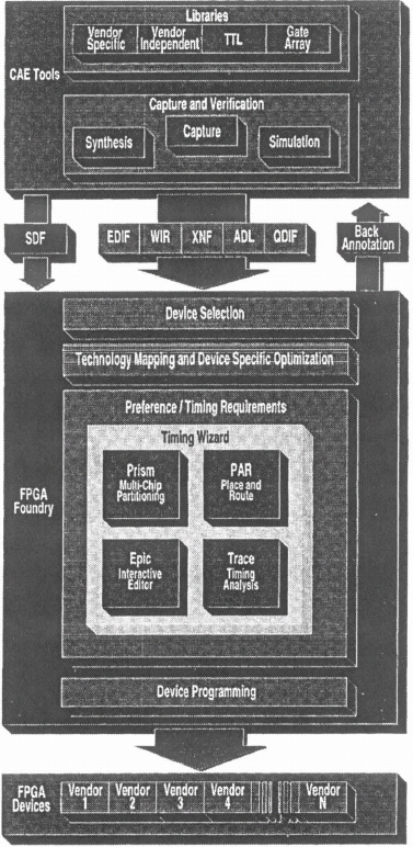
Figure 8–28. FPGA Foundry—design process flow.
Four interactive modules comprise NeoCAD’s timing-driven placement tools as shown in Figure 8–29. Auto Placement, the Delay Predictor/Scoring Function, Delay Calculator Timing Analysis and Auto Routing. The Delay Predictor/Scoring Function interacts with Auto Placement to yield a placement that has the best chance of conforming to the frequency/timing constraints. The results of placement and delay prediction feed the Auto Routing and Delay Calculator Timing Analysis modules to complete the design with maximum conformance to frequency and timing information.
A variety of proprietary placement algorithms are used in parallel with the delay estimator. As placement proceeds, the delay estimator calculates anticipated wire and component delays. The delay estimator is customized for each FPGA family, since each family is constructed with different component choices and routing resources. The scoring function then augments the information from the delay estimator and from the initial preferences file by calculating several weighted judgments for factors such as path delays, slack, density, alignment along routing resources, and total connection length. The scoring function operates in parallel with the placement algorithms and the delay estimator.
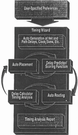
Figure 8–29. Timing Wizard—block diagram.
Timing Wizard determines the acceptability of a particular placement using inputs from the preferences list, the delay estimator, and the scoring function. A complete timing analysis is created based on actual delays of the routing paths chosen during placement. Timing analysis is conducted on two levels within the Timing Wizard: as a basis for placement and routing and as a standalone tool for postrouting analysis. Because the Timing Wizard comprehends frequency and timing constraints in the placement and routing process, most timing problems can be avoided.
The timing analysis package within Timing Wizard, called TRACE, is optimized for FPGAs. All the essential data for complex FPGA designs is provided, while irrelevant and extraneous information from typical timing analysis charts is edited for more efficient analysis by the designer. FPGA users can establish their own timing preferences as a filter, allowing TRACE to provide error reports for all results that do not meet the timing specifications. The error reports explicitly depict the path or net locations where problems exist, allowing quick identification and correction.
Partitioning When an FPGA design exceeds the capacity of even the largest device available, the design must be partitioned into multiple FPGA devices. Partitioning may also be required for cost or performance reasons. There are two categories of users who require the ability to partition their logic designs into more than one FPGA device—board-level designers and system-level ASIC designers—each with their own unique needs.
Unlike the traditional approach of dividing the design at the schematic capture level, PRISM partitions after technology mapping, allowing it to be truly timing driven, meeting user-specified operating frequencies and maximum point-to-point path delays. This is shown graphically in Figure 8–30. The tool operates within FPGA Foundry, providing a complete, integrated implementation environment. This is important, because timing-driven partitioning between devices cannot be effective without timing-driven place-and-route within each device.
PRISM is useful for both board-level designers and system-level ASIC designers. For those designing at the board level with multiple FPGAs, PRISM obsoletes the manual process by automatically generating a partition optimized for utilization and timing performance. Although PRISM can be used with little more than the desired operating frequency as input, the ability to manually specify numerous constraints or preferences, such as signals to split, signals not to split, and assignment of specified logic into target devices (floorplanning) is also fully supported. Even with careful manual partitioning, this level of optimization has not previously been possible.
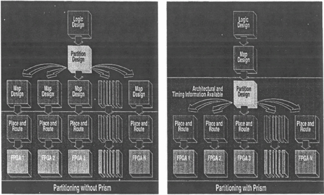
Figure 8–30. PRISM-pre-and post-mapped partitioning.
For system-level ASIC verification prototyping, PRISM not only eliminates the need for manual partitioning but also improves time-to-market for ASIC systems. This is because system-level ASIC verification can run in parallel with the later stages of design, verification, and fabrication. Since the prototype is designed and built by the designer, multiple copies can be made inexpensively. Further, PRISM’s timing-driven postmapped approach yields prototypes that run at optimum speed with less chance of internal timing problems. If major changes are made to the design, PRISM will determine if a new partition needs to be made and, if necessary, repartition while still adhering to timing requirements. PRISM supports incremental partitioning, which prevents it from repartitioning the entire design if only a small change is made.
PRISM is invoiced after completing technology mapping of the logic design (see Figure 8–30). The user provides PRISM with timing requirements and a list of the devices in which to implement the design (e.g., two Xilinx 3090s and a 3042). The user may select switches to control features such as incremental partitioning and the level of effort PRISM exerts, trading execution time for solution optimization.
PRISM then draws on technology-specific algorithms to determine the best partitioning solution for the design. PRISM uses an iterative loop of the following activities to develop the solution: generating a partition; evaluating it on the basis of the timing requirements, the number of interconnections, utilization of each device, and adherence to user-specified preferences or constraints; then improving the partition based on these results. This iterative loop is fully automatic, requiring no intervention from the user. Once the partition is generated, the resulting designs are ready for the remainder of the FPGA implementation tasks provided by FPGA Foundry.
PRISM is also fully integrated with Timing Wizard, NeoCAD’s advanced timing-driven tool that provides the user with complete control over timing requirements and operating frequencies during the implementation of FPGA designs. This integration from mapping and partitioning, through place-and-route, is crucial to providing a timing-driven solution that works. Since each of these functions contribute to the ability to meet the desired operating frequency, it is important that they all work from the same data, and that each software module is capable of meeting the user constraints and timing requirements delivered from the module preceding it. Working together, these automated tools can produce results equivalent to those of a dedicated, knowledgeable engineer, but in a fraction of the time.
HYDRA Client/Server Place-and-Route Engine The iterative placement and routing algorithms used by NeoCAD can optimize designs simply by allowing the process to run for longer periods of time. Multiple alternatives can also be explored to find the best solution to an FPGA design, including single- and multiple-chip designs. This process is computer-intensive and tends to consume substantial computer time.
HYDRA was designed to utilize the computing power available on networks that are typically not used during “off hours.” The two components of HYDRA, HYDRA Manager and HYDRA Place and Route, enable multiple, simultaneous placement and routing of FPGA designs to improve design completion rates and decrease overall implementation time. The HYDRA Manager provides automatic distribution of the place-and-route process to available network CPUs and serves as the control point. The user specifies the design parameters and available CPUs, and the HYDRA Manager allocates the design processing to appropriate CPUs. The HYDRA Place and Route modules accept mapped or previously placed and routed designs as input to explore alternatives that might yield improved designs.
CAE Tool Integration NeoCAD’s FPGA Foundry is fully integrated with CAE tools for design capture, logic synthesis, and simulation. Designers are free to choose the best front-end tools for their needs and to use the vendor-independent FPGA Foundry for their FPGA designs.
NeoCAD has adopted the industry-standard library of parameterized modules (LPM) as a standard library for FPGA design. This library includes both primitive and block-level functional components, and features parametric design specification to offer designers broad flexibility in creating designs. FPGA Foundry supports hardware description language (HDL) design and synthesis tools with architecture-specific logic optimization capabilities, timing-constraint interfaces to and from logic optimization and physical place-and-route, and hard-macro integration, both through automatic inference from HDL descriptions and explicit user instantiation. FPGA Foundry provides full simulation support with postlayout back annotation for accurate timing models.