
1.5 DESIGN METHODOLOGIES
1.5.1 Describing a Design
There are many ways of describing a design and confusion over what a design description is. Diagramming templates and drawing boards have been replaced by electronic computer-aided design (CAD) products. Technology progress and the resultant increases in design complexity have extended simple circuit descriptions in terms of transistors, resistors, and capacitors to data bases that can include hierarchical schematics, hardware description language programs, simulation models, layout artwork, test patterns, and so on. This plethora of design data can be understood more clearly by separating design description and notation. To describe a design unambiguously, data must be created, or generated, in three domains of description: structural domain, behavioral domain, and physical domain. Figure 1–17 shows a Venn diagram representation and identifies the elements of design description in each domain. At the logic level a structural description could be a logic diagram, a behavioral description could be a set of logic equations, and a physical description could be a standard cell layout for an ASIC (or a fuse map for a PAL). Appropriate notations are used to create these descriptions, while different notations may be used to create different fragments of design. A read-only memory (ROM) will appear as a block in a logic schematic with its contents in a truth table.
In addition, complex designs are created by building up design descriptions over a number of levels. Traditionally, engineering design has involved a divide and conquer approach in which conceptually large modules are partitioned into smaller units repeatedly until suitable for implementation at some (physical) level of design abstraction. Conceptual levels of design abstraction include circuit, logic, register transfer, and processor-memory-switch (PMS) [Bell71]. Physical levels of abstraction include semiconductor components, printed circuit boards, and card cage backplanes. So the one-dimensional view of design descriptions (Figure 1–17) is too simple and should be modified to allow for descriptions at different levels, each single domain becoming a multiple number of sheets. An elegant method of visualizing this, and any design process flow (see Chapter 4), has been suggested [Gajski88] in which a relational graph with three axes, a “Y”, is used for the three domains of description (Fig. 1–18). Each axis is scaled for level of design. With this diagram, design process steps can be represented by transitions (arcs) from a point on one axis to a point on another axis, such as creating a layout for a logic diagram. Design process flows thus appear as spiral paths toward the origin of the graph, as design process steps progressively refine behavioral, to structural, to physical design descriptions.
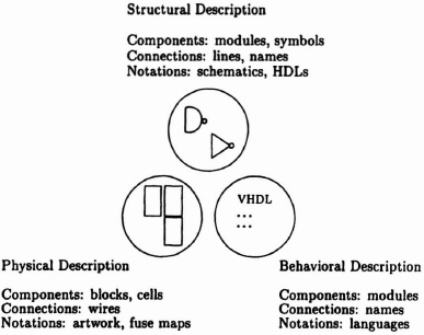
Figure 1–17. Domains of description.

Figure 1–18. Gajski–Kuhn diagram.
Structural Design Structural design simply connects elements together. It is common to most branches of engineering. Wires connect active and passive components in electronics, rivets and fasteners connect structural elements and beams in bridge building. In both cases, the structural composition defines an architecture that imbues the system it defines with certain desirable characteristics: performance, structural integrity, and so forth. A fuzzy, rather than precise objective in structural design, is to create an elegant architecture that addresses cost and performance objectives of the specification in a simple but effective way. With FPGAs, structural design is achieved with a schematic drawing tool.
Physical Design Physical design involves producing sufficient data for a design to be manufactured, including testing. With FPGAs, physical design requires the definition of functions for the logic blocks and routing paths for the interconnections. This is analogous to producing a layout in VLSI design. The manufacturing data are held in a binary file for programming the part. Tools used for physical design include symbolic editors, generators, automatic place-and-route software.
Behavioral Design Behavioral design is creating a description of the way in which the design functions. It may be embodied in a simulation model, a hardware description language program, a set of logic equations, or simply a truth table. Logic diagrams can become behavioral descriptions with the use of simple drawing conventions. PAL implementations are often developed by writing behavioral descriptions in proprietary hardware description languages.
1.5.2 Hierarchical Design
Hierarchical, or structured design, was rediscovered by hardware designers in the late 1970s, when the increasing complexity of full-custom design for products such as microprocessors created serious bottlenecks. Prior to this, software engineers had adapted traditional “divide and conquer” engineering methods in building complex software products. Ideas such as modularization, information hiding, stepwise refinement were recast to help VLSI design tasks. In effect, programming techniques were applied to VLSI layout design because programming language constructs allowed crisp descriptions of artwork, particularly when it contained iterated or conditional features. Whole software design products, including silicon compilers and generators, evolved at this time. The complexity levels of present-day FPGAs match the custom designs of that period, so that the ASIC design methods developed then remain highly relevant.
Figure 1–19 shows two hierarchical decompositions of a simplified datapath that could form part of a Von Neumann computer. The drawing could be expanded to a more detailed set of schematics which, at the lowest level, would show circuit or logic diagrams of cells. Both partitionings are valid design descriptions and they differ by choice of partitioning scheme: horizontal, emphasizing bit slice designs, or vertical, emphasizing functional unit designs.
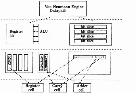
Figure 1–19. Hierarchical partitions of a datapath.
Just as there is a choice of partitioning scheme, there is also a choice in the expression of a wiring scheme. In this example, there would normally be bussed, that is, global, wires to communicate operands and results between the register file and the ALU. A true hierarchical design would partition pieces of these wires into the underlying cells, introducing a potential complexity in getting at connectivity data for simulation. There is an analogy here to the use/danger of global variables in software design.
1.5.3 Technology-independent Design
Technology-independent design asserts that it is desirable to design only at a high level, using a hardware description language (HDL), and have this converted automatically by synthesis software to an intermediate form that can be targeted to different implementation styles and different suppliers. It is analogous to high-level language compiler technology where code generators work from an intermediate form to create code for specific machines. The arguments for technology-independent design include increases in design productivity from working at a high level, and increases in optimality by having the broadest choice of supplier and ASIC solution, not to mention the avoidance of being in thrall of a single supplier. Arguments against technology-independent design include loss of efficiency in mapping a high-level design to an implementation and the associated loss of direct control of time and space in a design, both of which may be key to a winning implementation. The current battle-ground for these arguments is the FPGA marketplace. Technology-independent and gateless design are possible with the appropriate toolset. Decisions relative to the cost in space and speed are left to the design engineer responsible for the application. In engineering in general, irrespective of the level of design, it has always been the case that great designs can be an order of magnitude better than average designs, most usually because of the creative insights of an engineer with an understanding of the underlying technology, that is, technology dependence.
1.5.4 The Mead–Conway Design Method
In 1980 a text appeared [Mead80] that described a methodology for VLSI design down to the silicon artwork level. The techniques advocated have been widely adopted in the design of large silicon structures. The described methodology is state of the art and is embodied in software products for design. Mead–Conway (for lack of a more descriptive name) is a hierarchical design method that places emphasis on managing the communications (wiring) complexity in a design. This is important, since the cost of moving data around a VLSI circuit is at least as large as the cost of working on it. Mead was one of the first to understand this and propose efficient design techniques, which include:
- Wiring management as a key objective in high levels of design.
- Use of simple design rules to abstract away detail.
- Use of building blocks as in data paths and PLAs (two-level logic blocks) that have “naturally” elegant wiring structures (see Table 1–3).
This methodology places emphasis on structural and physical aspects of design in transforming architectural specifications like Figure 1–13 to clean implementations as in Figure 1–20. There are obvious isomorphisms in the descriptions. In fact, the Mead–Conway methodology normally keeps the structural and physical descriptions isomorphic, thus avoiding the complexity pitfall in hierarchical design of having separate structural and physical hierarchies. Using a program to generate both hierarchies, for example, a silicon compiler, is a convenient way of keeping descriptions consistent.
TABLE 1–3. Natural Wiring Forms
| Module | Natural Form |
| Logic function | Two-level logic block (PLA, ROM) |
| State machine | Two-level logic block (PLA, ROM) |
| Register file ALU Multiplier |
Data path Data path Combinatorial array |
With FPGAs, all of these techniques can be applied, provided the FPGA delivers a homogeneous implementation medium for building circuits. In this respect, the fine-grain FPGA architectures, like the Configurable Logic Array with its cellular array of gate level elements, are a better match to a homogeneous environment than coarse-grain channeled architectures. The former can be expected to provide alternative implementation options for VLSI designers.
1.5.5 Temporal Design
With FPGAs, or any implementation medium, there are decisions to be made about the time domain aspect of the design. These decisions are largely in the area of choice of timing discipline and design for performance. The provision of specific types of storage elements in the basic cell of the FPGA may restrict the choices open to the designer.

Figure 1–20. Reduced Instruction Set Computer (RISC) processor datapath. (Photograph courtesy of P. Crockett.)
Clocked In this discipline the actions of individual cells are synchronized to a system clock. It helps to consider a circuit as a sequence of register transfer computations, as in Figure 1–21. Timing disciplines impose a regulated data flow through the system so that intermediate results are held safely in registers after being computed by one stage of combinatorial logic and before being passed on to the next stage of combinatorial logic. The usual analogy is between this model and the locks of a canal. If two consecutive registers/“lock gates” are open in the same period of time, data/“water” will “flood” through the system. Problems can arise when delays on the wires distributing the clocks skew these signals and shift the register operations in time. Some FPGAs provide special global, low-delay wires to ensure synchronous operation.
If FPGA cells are to be used as “smart-memory” within a computer system, then a clocked scheme may be the technique of choice, since it allows a microprocessor to read and write to internal nodes of a circuit implemented by the cells without disturbing a computation being performed by the cell array. Note that the choice of a clocked system does not relieve the user of responsibility for removing timing hazards.
Single-phase clocking: One way to ensure correct operation is to use edge-triggered master–slave storage elements and a single-phase clock (clocks 1 and 2 in Figure 1–21 would be the same signal). This discipline, defined in the TTL era, is supported by such storage elements in FPGA families.
Two-phase clocking: Another method of ensuring correct operation is to use two-phase nonoverlapping clocks with storage latches. This would apply in Figure 1–21, and the lack of overlap between clock 1 and clock 2 prevents data moving more than one stage per clock cycle. This timing discipline was popularized during the VLSI era and is described in [Mead80]. In some situations, for example, if the FPGA provides latches with true and complement clocks, it is possible to avoid the extra wire overhead and use a single clock feed.

Figure 1–21. Register transfer model.
Self-timed In this discipline, described by Seitz in [Mead80], each cell generates explicit “go” and “done” signals which are routed in parallel with the data signals. An edge transition, up or down, is a handshake signal, and any time may elapse between transitions. This discipline is very attractive since it relieves the user of most of the timing problems associated with logic design. However, if one were to build a purely self-timed FPGA there could be an area cost, since the cell logic is more complex than for a synchronous methodology. The “go” and “done” signals take routing resources, and fairly large “consensus” gates are required where wires split at multiplexors and where functions are being computed to provide the necessary control.
In the case of self-timed micropipelines there can be efficient FPGA implementations with conventional cell resources. Chapter 6 gives two examples.
1.5.6 Pipelined
This is an extension of the clocked design methodology and offers some exciting possibilities. If all transfers within and between cells are synchronized to a single, fast system clock and additional buffer storage is provided at each selection position, then the system can be pipelined at a very low level. The storage requirement does not imply an unacceptable overhead because of the storage by the gate capacitance of the buffering inverters.
1.5.7 Unsynchronized
In this case, users are provided only with logic gates and take full responsibility for timing themselves. This flexibility is necessary for cells that are to be used as PLDs.
PROBLEMS
1. How big should a PCB be?
2. What is best way to make wiring capacity match wiring demand, for example, with a PCB?
3. Structure a “flat” design in two different ways.
4. Structure/partition a design for FPGA implementation.
5. Do a design selecting components from a library selection and then in free form.
6. What happens to global wires in a hierarchical design? What implications does this have for different design processes including: schematic design, layout, and simulation?
BIBLIOGRAPHY
[Altera92] Data Book, Altera Corporation, 1992.
[Bell71] Bell, C. G., Newell, A., Computer Structures: Readings and Examples, Addison-Wesley, 1971.
[Bell72] Bell, C. G., Grason, J., Newell, A., Designing Computers and Digital Systems Using PDP-16 Register Transfer Modules, Digital Press, 1972.
[Bell78] Bell, C. G., Mudge, J. C., McNamara, J. E., Computer Engineering: A DEC View of Hardware Systems Design, Digital Press, 1978.
[Bell91] Bell, C. G., McNamara, J. E., High-Tech Ventures—The Guide for Enterpreneurial Success, Addison-Wesley, 1991.
[Cavlan75] Cavlan, N., Cline, R., “Field-PLAs Simplify Logic Design,” Electronic Design, pp. 84–90, September 1975.
[Chan94] Chan, P. K., Mourad, S., Digital Design Using Field Programmable Gate Arrays, Prentice-Hall, 1994.
[Fawcett92] Fawcett, B. K., “Taking Advantage of Reconfigurable Logic,” The Programmable Gate Array Data Book, Xilinx, Inc., San Jose, pp. 7-24–7-32, 1992.
[Gajski88] Gajski, D. D., Silicon Compilation, Addison-Wesley, 1988.
[Gray79] Gray, J. P., “Introduction to Silicon Compilation,” Proc. 16th Design Automation Conference, pp. 305–306, June 1979.
[EDN92] Anon., “High-Density PLDs,” EDN, pp. 76–88, January 2, 1992.
[Laws90] Laws, D. A., “Programmable Logic Is In!” Electronic Engineering Times, p. 52, August 20, 1990.
[Mead80] Mead, C. A., Conway, L. M., Introduction to VLSI Design, Addison-Wesley, 1980.
[Patter93] Patterson, W., “A Flood of New Programmable Logic Devices,” Xcell, No. 9, pp. 3–5, 1993.
[Swager92] Swager, A. W., “Choosing Complex PLDs and FPGAs,” EDN, pp. 74–84, September 17, 1992.
[TTL88] TTL Logic Data Book, Texas Instruments, 1988.
[Xilinx92] The Programmable Gate Array Data Book, Xilinx, Inc., 1992.