
2.5 ELECTRICAL ASPECTS
While from many points of view we may regard FPGAs as consisting of idealized logic elements, in practice we need to be aware of the ways in which they are realized as electrical circuits, and their operation as analog circuits.
2.5.1 Complementary MOS Circuits
Almost all FPGAs use CMOS integrated-circuit technology. It uses two types of MOS transistor, referred to as N- and P-type. N-type transistors employ electrons as mobile charge carriers, while P-type transistors use holes instead. Figure 2–16 shows a complementary pair connected to form an inverter. Since we know that holes will move toward a lower potential and electrons toward a higher one, we can label the source (S) and drain (D) terminals as shown. The N-type transistor conducts if the voltage between its gate (G) and source exceeds a small positive threshold voltage. The P-transistor conducts if its gate-to-source voltage is more negative than a small (negative) threshold voltage. So if the input voltage to the inverter is zero (logic false), the P-transistor conducts, while the N-transistor does not. This causes the output voltage to be raised to the supply voltage Vdd, by charging the output capacitance. If the input voltage is high, corresponding to logic true, the N-transistor conducts, discharging the output capacitance and producing a logic false value. CMOS output voltages swing between the full range of the supply rail voltages, and can tolerate significant deterioration in input logic levels. As a result CMOS circuits have excellent noise margins.

Figure 2–16. CMOS inverter.
Either type of transistor may be used as a voltage-controlled switch, referred to as a pass transistor. While conduction can take place in either direction, since the roles of source and drain reverse, an N-transistor will only conduct while its gate–source voltage exceeds its built-in threshold voltage, and similarly the P-transistor in the complementary sense. Accordingly, an N-transistor can be described as a “good conductor of 0s, but a poor conductor of 1s,” and vice versa for its P-type counterpart. Degradations in signals are corrected with active logic such as the inverter just described. While pass transistors take little space, they introduce significant capacitance to ground and have finite series resistance, for example, 1–10 kilohms when conducting. The effect on signal propagation speeds is discussed later in this chapter.
2.5.2 Voltage Levels and Loading
FPGAs may be used with other CMOS circuits and also TTL circuits. The power supply voltage is 5 V, and so CMOS output voltages swing from 0 to 5 V. TTL circuits have a smaller output voltage range, typically from 1 to 2.5 V. Some FPGA pad circuits can be configured for this range of input signals as well as for CMOS.
Inside an FPGA, circuit loads consist of capacitances that are charged and discharged. There is very low power dissipation when there is little activity, a particularly strong feature of CMOS circuits. As clock frequencies are increased, the power dissipation may become quite significant.
2.5.3 Three-state Outputs
A three-state driver circuit* is controlled by two signals—an enable/disable signal that allows the other signal—high or low, to be applied to the output being driven. If disabled, the output is effectively disconnected from the input, and may float or be driven to a logic high or low level by an enabled driver connected to the same output, typically a bus connection. The third state is referred to as the high-impedance state. As well as providing three-state pad drive capabilities, some FPGAs contain internal three-state buses, which allow many-input AND functions.
2.5.4 Signal Propagation in CMOS
Modem CMOS processes provide a number of alternative conductors for interconnections. Typically there are two, or sometimes three metal layers, which have low series resistance and low shunt capacitance to the substrate. These are excellent for propagating signals over (relatively) long distances, for example, a clock that must feed many different parts of an FPGA with very little skew, that is, variation in arrival times. To provide flexibility in interconnection, reprogrammable FPGAs use MOS transistors as switches between conductors, each controlled by a static RAM bit. The transistor introduces much more resistance and capacitance, as well as degrading the signal somewhat. In consequence, complex connections may have significant amounts of resistance and capacitance distributed along their length. The resulting circuit may be analyzed as an R–C transmission line [Weste93]. For a truly distributed line, a partial differential equation known as the diffusion equation applies. Analysis shows that signal propagation times increase as the square of line length. In consequence, FPGAs often use buffer amplifiers to break such interconnections into sections with short delay. Provided the buffer delays are small, the overall delay can actually be reduced, but this adds a further complication in that connections are no longer bidirectional, and buffers must be configured to take into account signal direction.
2.5.5 Electrostatic Precautions and ESD Protection
Particularly in dry climates, it is easy to generate voltages of the order of several thousand volts by electrostatic effects, such as friction with an insulator. If handled carelessly such voltages may be applied to an integrated circuit chip and cause it to fail. Fortunately, FPGA chips are equipped with electrostatic discharge (ESD) protection circuits, which limit the effect of such voltages. Despite these protection mechanisms, users should employ electrostatic discharge mats and wrist ground straps when handling FPGAs or any CMOS integrated circuit.
2.5.6 Switch Debouncing
Mechanical switches are not ideal in their behavior. For example a single-pole, single-throw switch such as in Figure 2–17, will exhibit contact bounce when operated, that is, the moving contact will momentarily be connected and within milliseconds be disconnected, possibly making several brief contacts before settling down. Logic circuits are so fast that they don’t distinguish switch bounce from deliberate user actions. The circuit shown in Figure 2–18 uses a set–reset flip-flop to “remember” the first connection, and provided the switch doesn’t make contact with the upper contact again, will cause the signal OUT to make a single transition from ground to Vdd.
2.5.7 Power Supply Regulation
FPGA chips usually have multiple numbers of Vdd and ground connections, to ensure that power supply voltage levels are maintained inside the chip. Switching rates are often so high that quite large instantaneous currents flow in the power supply connections, both on- and off-chip. Although inductive effects are negligible inside the chip, the small inductance of the circuit package and connecting wires or traces can lead to significant voltage drops in power supply connections. Some FPGA output circuits can be configured to be slew-rate limited, provided the associated signals do not have to be fast changing for the application. This can have beneficial effects, both on power supply regulation and in reducing noise.
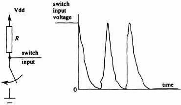
Figure 2–17. Switch contact bounce.
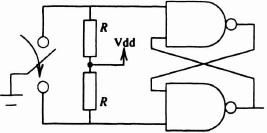
Figure 2–18. Debounced switch circuit.
2.5.8 Metastability Characteristics
The theory of synchronous sequential circuits assumes that all signals, whether external or internal, are stable during a “decision window” around the time of clock transitions. The manufacturer of any flip-flop specifies setup and hold times before and after the clock edge, as illustrated in Figure 2–19, during which the input signals, such as D, should be stable, along with a propagation delay for any output change, Q. Many systems have to cope with real-time inputs that are not synchronized to the system clock, and so this requirement cannot be guaranteed. If an input changes within the decision window defined by these values, the effect may be to cause the flip-flop to change state, but with insufficient energy to make a complete transition. If a partial transition takes the flip-flop output voltage to a central region midway between the supply rail voltages, there may be little or no feedback to complete the transition or return to the previous state.
Consider the experiment suggested by Figure 2–20. The logic threshold voltage Vinv is that for which the input and output voltages are identical. Given identical inverters, if we set the upper input voltage to Vinv and closed the switch before removing the voltage source, the circuit would remain poised at Vinv forever! This only appears to be a stable state, since the slightest disturbance is reinforced by positive feedback around the loop and drives the circuit voltages to stable values, high or low. Accordingly the third state is referred to as metastable. The longer we wait after a clock edge, the more likely the output will have reached one of the true stable states, but we can only express this in terms of probability. Theoretical and experimental studies have confirmed this phenomenon and related it to parameters that can be determined for any flip-flop.

Figure 2–19. Metastable behavior of a flip-flop.
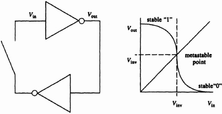
Figure 2–20. Metastable operation.
Assume that the clock rate is fc and the D input experiences asynchronous edge transitions uniformly distributed over the clock period at a lower frequency f. We will not see any change in the flip-flop output until the nominal propagation delay tp is over. If we wait a given time tr (measured from the rising clock edge), we will occasionally find that the Q output is neither a good “0” nor a good “1,” that is, it is metastable. The mean time between such events will be
![]()
where T0 and τ are constants for the flip-flop concerned, assuming operation at f, fc Figure 2–21 shows the improvement brought about by a few nanoseconds of extra delay for an internal flip-flop of a particular FPGA. It is based on [Alfke92] and includes the nominal propagation delay. Fortunately, the small size and high speed of flip-flops realized internal to FPGAs has considerably improved the situation, compared with earlier small-scale integration (SSI) parts.
Although metastability cannot be eliminated for synchronous systems subject to asynchronous inputs, its effects can be reduced by
- keeping clock frequencies as low as possible
- using a synchronizer for each asynchronous input
- using extra clock cycles for resolution

Figure 2–21. Improvement in metastability resolution with added delay.
All these points delay the processing of data slightly, but the alternative of unreliability is unacceptable. Reference [Shear92] discusses some improved synchronizers.
PROBLEMS
- You have been given a state diagram for a sequence checker, whose output will be 1 whenever the sequence 0101 is detected. Develop a one-hot design that takes advantage of possible simplifications. Specify the state transition table. The design should use D flip-flops and combinational logic restricted to NANDs, NORs, and inverters.
BIBLIOGRAPHY
[Alfke92] Alfke, P., Wu, P., “Metastable Recovery,” The Programmable Gate Array Data Book, Xilinx, Inc., pp. 6-16-6-17, 1992.
[Dingman91] Dingman, S., “Determine PLD metastability to derive ample MTBFs,” EDN, pp. 147–154, August 5, 1991.
[Hill93] Hill, F. J., Peterson, G. R., Computer Aided Logical Design With Emphasis on VLSI, 4th ed., Wiley, 1993.
[Johnson93] Johnson, H. W., Graham, M., High-Speed Digital Design: A Handbook of Black Magic, PTR Prentice-Hall, 1993.
[Knapp90] Knapp, S. K., “Accelerate FPGA Macros with One-Hot Approach,” Electronic Design, September 13, 1990.
[Leach93] Leach, T., Hackett, B., “Modem Synchronous Design,” ASIC & EDA, ASIC and EDA, Los Altos, pp. 44 and 50–52, 1993.
[Mead80] Mead, C. A., Conway, L. M., Introduction to VLSI Systems, Addison-Wesley, 1980.
[Murata89] Murata, T., “Petri Nets: Properties, Analysis and Applications,” Proc. IEEE, Vol. 77, No. 4, April 1989.
[Peterson81] Peterson, J. L., Petri Net Theory and the Modeling of Systems, Prentice-Hall, pp. 195-196, 1981.
[Petri87] Petri, C. A., Concurrency Theory: Petri Nets: Central Models and Their Properties, Advances in Petri Nets 1986, Part 1, W. Brauer, W. Reisig, and G. Rozenberg, Eds., Springer, pp. 4–24, 1987.
[Schlag91] Schlag, M., Chan, P. K., Kong, J., “Empirical Evaluation of Multilevel Logic Minimization Tools for an FPGA Technology,” FPGAs, Edited Papers from the International Workshop on Field Programmable Logic and Applications, W. Moore and W. Luk, Eds., pp. 201–213, Abingdon EE & CS, 1991.
[Shear92] Shear, D., “Exorcise Metastability from Your Design,” EDN, Vol. 37, No. 25, pp. 58–64, December 10, 1992.
[Shoji92] Shoji, M., Theory of CMOS Digital Circuits and Circuit Failures, Princeton University Press, Princeton, 1992.
[Unger86] Unger, S. H., Tan, C. J., “Clocking Schemes for High-Speed Digital Systems,” IEEE Transactions on Computers, Vol. C-35, No. 10, pp. 880–895, October 1986.
[Wakerly90] Wakerly, J. F., Digital Design Principles and Practices, Prentice-Hall, 1990.
[Weste93] Weste, N., Eshraghian, K., Principles of CMOS VLSI Design, 2nd ed., Addison-Wesley, 1993.
*Carver A. Mead and Lynn Conway, Introduction to VLSI Systems (pg. 85), ©1980 by Addison-Wesley Publishing Company, Inc. Reprinted by permission of the publisher.
*Section 2.4 was contributed by Erik L. Dagless, Jonathan M. Saul, and Tomasz Kozlowski.
*This example is based on traffic signaling practice in the United Kingdom.
*The term Tri-State is sometimes used instead. Tri-State is a trademark of National Semiconductor Corporation.