
8.2 NEW ARCHITECTURES
The chapter opens with some new FPGA architectures for reprogrammable FPGAs. We have deliberately excluded fuse- and electrically programmable FPGAs. Readers may note the wide range of approaches at both ends of the spectrum from fine- to coarse-grain, and the importance of wire delays—dynamic reprogrammability does not come for free. It is interesting to note that “dynamic” includes the possibility of reconfiguration while FPGA logic is active. Until recently virtually all manufacturers chose a serial loading process which implied that any change required a total reconfiguration, even for a single bit. Clearly most present-day applications do not require truly dynamic reconfigurability, but new applications may well exploit it, and this will require total reconsideration of CAD support and the host environment in cases where the FPGA is interfaced to a host computer.
8.2.1 Altera FLEX
Altera has developed four generations of complex programmable logic devices (CPLDs). The various families of devices are Classic, MAX 5000, MAX 7000, and FLEX 8000. While there are many differences in architectural details of these three families, there are some significant similarities as well. The similarities are a rich (nonblocking, local/global) interconnection scheme, and a coarse-grain/fine-grain logic architecture (groups of logic elements in clusters called logic array blocks (LABs)). The following is a brief description of the FLEX 8000 family.
FLEX 8000 The FLEX 8000 family is fabricated using a standard complementary metal-oxide semiconductor (CMOS) technology. Static random-access memory (SRAM) bits are used as the programming element. Semiconductor technology aside, there are other details of the FLEX architecture that are different from the earlier Classic and MAX families. However, the common heritage of LABs (fine-grain/coarse-grain logic architecture) interconnected by a hierarchical interconnect structure is apparent.
Dual Granularity A macroscopic view of the FLEX architectures is shown in Figure 8–1. Logic elements (LEs) are grouped in clusters of eight to form LABs. Within a LAB, the output of every LE is available as an input to every other LE by means of a completely nonblocking local interconnect scheme (Local FastTrack). The grouping of LEs into LABs enables the FLEX 8000 devices to exhibit the high-speed characteristics of coarse-grained architectures together with the high logic utilization of fine-grained architectures.
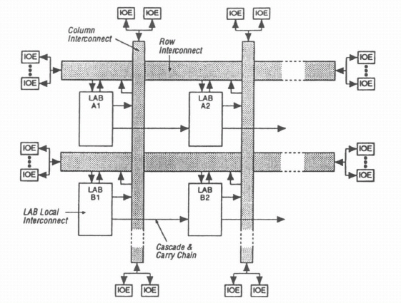
Figure 8–1. FLEX architectures.
Logic Array Block LABs communicate with other LABs by means of row and column interconnect buses called FastTrack. These are continuous metal lines that span the chip, horizontally and vertically, eliminating the highly variable, cumulative delays of the segmented interconnect structure commonly found in FPGAs. The FastTracks are also used to carry signals to and from the input/output elements (IOEs).
Signals enter a LAB from the Row FastTrack. Signals generated by a LAB are output to both the Row and Column FastTrack. Figure 8–2 shows a typical LAB in greater detail. There is a LAB Local Interconnect consisting of 24 lines selected from the Row FastTrack and 8 lines fed back from the output of each of the LEs within a LAB. In addition, there are 4 other inputs that provide clock, clear, and reset signals to the LE.
Logic Element The Logic Element, shown in Figure 8–3, is the smallest unit of logic in the FLEX 8000 architecture. Each LE contains a 4-input lookup table (LUT), a programmable flip-flop, a carry chain, and a cascade chain. For a purely combinational function, the flip-flop can be bypassed. The carry chain provides a very fast (<1 ns) carry-forward function between adjacent LEs. This feature allows implementation of high-speed counters and adders.
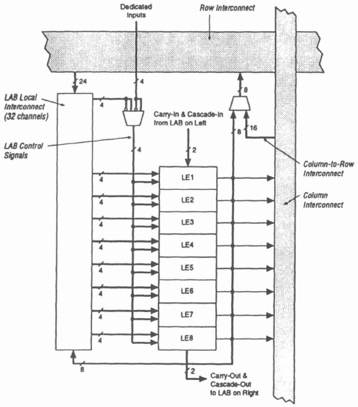
Figure 8–2. FLEX 8000 LAB architectures.
The cascade chain allows implementation of functions requiring wide fanin (wider than the four inputs of the LUT). Adjacent LUTs can be used to compute portions of the function in parallel; the cascade chain serially connects the intermediate values. Outputs of adjacent LUTs can be combined with either an AND or an OR function. Each additional LE provides four more inputs to the effective width of the function with a delay of approximately 1 ns per LE.
Input/Output Element Figure 8–4 shows the IOE block diagram. Signals enter the FLEX 8000 device from either the input/output (I/O) pins that provide general-purpose input capability or the four dedicated inputs that are typically used for fast, global control signals. The IOEs are located at the ends of the row and column interconnect.
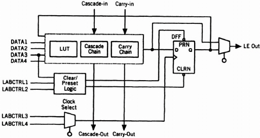
Figure 8–3. FLEX 8000 logic element.
I/O pins can be used as input, output, or bidirectional pins. Each I/O pin has a register that can be used either as an input register or as an output register. A programmable inversion option is provided to invert signals from the row and column interconnect when required. The output buffer also has an adjustable output slew rate that can be configured for low-noise or high-speed performance.
The Clock, Clear, and Output Enable controls for the IOEs are provided by a network of I/O control signals. These signals can be supplied by either the dedicated input pins or internal logic. The IOE control signal paths are designed to minimize the skew across the device. All control signal sources are buffered onto high-speed drivers that drive the signals around the periphery of the device. The I/O control signals can be configured to provide up to ten Output Enable signals, and up to two Clock or Clear Signals.
The FLEX Family The current family of FLEX 8000 products is shown in Figure 8–5. The FLEX family brings high register counts and high performance together in one programmable logic family. The FLEX 8000 family consists of devices in six logic densities that range from 2500 to 16,000 usable gates. Total flip-flops in the device family range from 282 to 1500. In addition, a variety of pin count options, from 84 to 304 leads per device, are well-suited for a wide range of I/O intensive applications.
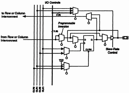
Figure 8–4. FLEX 8000 I/O element block diagram.
The FLEX 8000 family builds on Altera’s previous innovations found in the Classic, MAX 5000, and MAX 7000 families of programmable logic devices. The result is a logic family that combines the high speed, predictable timing, and ease of use of EPLDs, with the high register counts, low power consumption, and in-circuit reconfigurability normally associated with FPGAs.
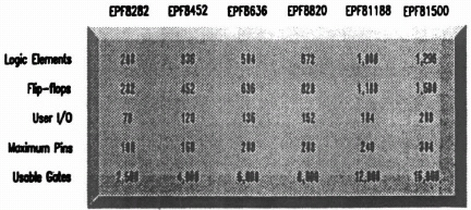
Figure 8–5. FLEX 8000 family of products.
8.2.2 Pilkington (Motorola/Plessey/Toshiba)
The PMeL FPGA architecture is currently in its fourth generation. This development process has taken place over a 6-year period. During this time PMeL has gained a wide body of experience in the techniques required to obtain the high performance and capacities needed from a leading-edge FPGA and an understanding of the users’ requirements from such devices, particularly in the field of autolayout software. This is an area often neglected, especially for fine-grain architectures where the problem may be difficult. The focus of the development effort has been to produce an architecture that works in sympathy with the autolayout software to produce a complete design system. Advanced architecture development tools have allowed the architecture and autolayout algorithms to be developed simultaneously. The Pilkington FPGA architecture is currently under license to Motorola Inc., Toshiba Corporation, and GEC Plessey Semiconductors.
The Pilkington Micro-electronics Architecture The Pilkington architecture is based on a sea-of-gates structure. All function elements (cells) directly abut, unlike the more common channeled-FPGAs (e.g., Xilinx, Actel) where there are routing channels separating the cells. The close proximity of functional cells allows fast direct connections between neighboring cells, enabling the user to combine cells to form compact local functions. A hierarchical routing network runs over the top of the array, making highly efficient use of the available silicon area. All cells implement only simple functions, allowing the basic cell to be optimized for performance.
The Array Structure A key feature of the Pilkington array is its provision of a hierarchy of resources, both for function and interconnect. Although it is modeled on a sea-of-gates type, a flat array of this type was found to be an inefficient target for autolayout. It forces the tools to treat autolayout as one simultaneous and very complex problem. A better solution is to break the problem into simpler subproblems. This is achieved by partitioning the array into 100 cell zones (see Figure 8–6). Each zone can then be treated as a separate autolayout problem. A zone can be considered as a separate array with the port cells forming an interface between the zone interconnect and the global interconnect, see Figure 8–7. The global interconnect joins individual zones together to form the larger array. There is also a hidden clock network which distributes very low skew clocks throughout the array, directly into cells that have clocked registers.
The Interconnect The structure of the interconnect also follows a strict hierarchy of resources. At the lowest level the fast local connections (see Figure 8–8), are used to join local cells to form macros. These efficiently implement small functions, such as a counters, comparators, and complex combinatorial functions. These functions are then combined, using the medium interconnect within the zone and the higher level global interconnect throughout the array, to construct the complete layout. The short range of the local connections and their limited loading means that they are very fast. As a result of this there is negligible overhead in building local function from individual cells. Additionally there is no redundancy in the cells used to construct the functions.

Figure 8–6. A 10,000-cell array.
The partitioning introduced into the array enforces a hierarchy onto the routing resources, with the port cell separating the zone routing resource and the global routing resource, see Figure 8–9. This separation enables the global and zone routing phases to be completed independently. The separation of the two layout phases allows the global partitioning and routing to be completed before any detailed zone-level layout has been done. This is a particular advantage when applying timing-driven autolayout algorithms to the array. Once the global layout phase has been completed an accurate estimate of the final layout performance can be made. This estimation allows realistic target delays to be assigned to the zone-level net while still obtaining the best possible performance from the array. Setting reasonable target delays for the zone-level layout results in consistent autolayout completion rates and shorter run times.
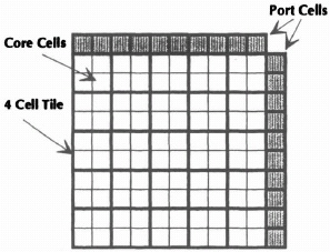
Figure 8–7. A 100-cell zone.
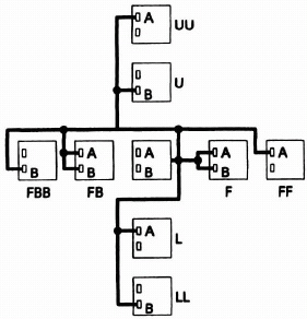
Figure 8–8. Local routing resources.

Figure 8–9. Resource hierarchy.
The hidden clocking structures provide an extra layer of interconnect which can be ignored by the autolayout process, further simplifying the task.
The Cell Another difference between this architecture and the current dominant architectures is the functionality of the cell. The cell used has a very low level of functionality, providing only a small set of two input functions. Using a conventional channeled routing structure, such a cell would be very inefficient with a high routing overhead between each level of logic; however, using a hierarchical routing structure, these small cells can be very efficiently combined into macros with negligible routing overhead. This combination has two main advantages: first, there is no redundancy; if a cell is only used to perform a simple function, there is no unnecessary capability in the cell to be wasted. Second, the simple cell can be very highly optimized, as the critical paths through the cell are limited in number.
The function of the cells on the array is no longer homogeneous, but varies over a group of four cells. This group of cells (a tile, see Figure 8–10) is then repeated uniformly over the array. The functions within each cell are simple fixed functions. All cells have a basic AND function along with a subsidiary function such as an XOR or D-type flip-flop. These subsidiary functions are available in the ratios found in typical gate array designs and are arranged in such a way as to allow the construction of very high performance hard macros. The tile is repeated uniformly across the array. The sharing of all the essential functions over a tile of four cells results in a significant improvement in the overall silicon efficiency, without any reduction in the gate count supported by the array. This is largely due the careful choice of the function ratios. The addition of a programmable inversion on the inputs to the cell extends the functions available and removes the need to consider net sense during the autolayout.

Figure 8–10. The 4-cell tile.
The Benefits The fine-grained structure of this architecture lends itself well to automated design and layout, and has been designed specifically with this in mind. The low-level nature of the basic element results in good performance across a broad range of applications, since there are no special complex structures. Where arrays use larger basic elements the performance is directly related to the ability of the design tools to map the application efficiently to the array elements. Inevitably this process will be more successful for some applications than others, leading to unpredictability in performance. This architecture is a particularly good target for synthesis tools, supporting all the fundamental functions required. As single levels of logic are supported within the cell, all nodes in a circuit are accessible. This gives the tools far greater flexibility, allowing areas to be optimized without compromising performance.
Dynamic Reconfiguration Any array programmed using volatile means can be used for dynamic reconfiguration in its basic form, that is, where the entire array is reprogrammed. However, the overhead required for this, that is, large data sets for each configuration and long configuration times, means that this form is not suitable for a large number of applications. The obvious enhancement is to partially program the device, thus reducing the size of the configuration data used and hence the time taken to reprogram it. When using a device in this mode there will be several independent functions resident on the array simultaneously. These functions will communicate with each other or the I/O. In either case if one of the functions is changed it must not alter the existing functions or their associated global routing. This is particularly a problem, since a complete rectangular area of the array must be programmed in order to use an efficient addressing mechanism.
The hierarchy of the Pilkington architecture directly supports the isolation of areas suitable for partial reconfiguration. As stated earlier the zone can be treated as an independent array and similarly, several zones can be grouped and treated as an independent area. By defining ports on this area, the layout inside can be swapped without affecting any of the existing global routing in the remainder of the array or interacting with any other existing function. A further advantage is that layouts defined in this way are position-independent, since all zones are identical.
8.2.3 Xilinx XC4000 Family
The XC4000 family of Field Programmable Gate Arrays is Xilinx’s third-generation static-memory-based FPGA architecture. As with the earlier XC2000 and XC3000 families, the architecture is based on three major configurable elements: a matrix of configurable logic blocks (CLBs), a perimeter of input/output blocks (IOBs), and programmable routing resources. The third generation XC4000 family extends this architecture, with a yet more powerful and flexible logic block. I/O block functions, interconnection options, and integration features have also been enhanced with each successive generation, further extending the range of applications that can be implemented with FPGA technology.
Configurable Logic Blocks A number of architectural improvements contribute to the XC4000 family’s increased logic density and performance levels. Principal among these is a more powerful and flexible configurable logic block (CLB) surrounded by a rich set of routing resources, resulting in more “effective gates per CLB”. Figure 8–11 is a block diagram of the principal elements within the XC4000 CLB.
Each CLB contains three combinatorial function generators, two flip-flops, and their associated control logic. Thirteen CLB inputs and four CLB outputs provide access to the function generators and flip-flops from the programmable interconnect lines surrounding the block. Four independent inputs are provided to each of two lookup-table-based function generators (F′ and G′). A third function generator, labeled H′, can implement any Boolean function of its three inputs: the functions F′ and G′ and a third input from outside the block (H1). In addition, each CLB contains dedicated arithmetic logic for the fast generation of carry and borrow signals (not shown in Figure 8–11); this logic is used in conjunction with the F′ and G′ function generators to implement high-performance arithmetic functions. The two storage elements in the CLB are edge-triggered D-type flip-flops with common clock (K) and clock enable (EC) inputs, a third common input (S/R) that can be programmed as either an asynchronous set or reset signal, and programmable clock polarity.
The flexibility and symmetry of the CLB architecture facilitates the placement and routing of a given application. Since the function generators and registers have independent inputs and outputs, each can be treated as a separate entity during placement to achieve high packing densities. Inputs, outputs, and the functions themselves can freely swap positions within a CLB during placement and routing operations.
CLBs and On-Chip Memory The XC4000 family FPGAs are the first programmable logic devices to include on-chip static memory resources, further increasing system integration levels. An optional mode for each CLB allows the memory look-up tables in the F′ and G′ function generators to be used as either a 16 × 2 or 32 × 1 bit array of read/write memory cells. Groups of CLBs can be used together to form a memory array of the desired length and width. Configuring the CLB’s function generators as read/write memory does not affect the functionality of the other portions of the CLB, with the exception of the redefinition of the control signals.
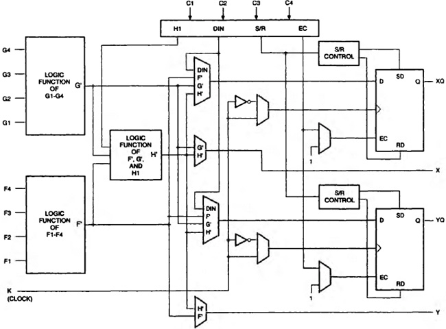
Figure 8–11. A simplified block diagram of the XC4000 Configurable Logic Block (CLB).
Input/Output Block User-configurable I/O Blocks (IOBs) provide the interface between external package pins and the internal logic (Figure 8–12). Each IOB controls one package pin and can be defined for input, output, or bi-directional signals. Input signals can be routed to an input register that can be programmed as either an edge-triggered flip-flop or a level-sensitive transparent latch. Optionally, the data input to the register can be delayed to compensate for the delay on a clock signal that first passes through a global buffer before arriving at the IOB, thereby eliminating any hold time requirement on the data at the external pin.
Output signals can pass directly to the pin or be stored in an edge-triggered flip-flop. Optionally, an output enable signal can be used to place the output buffer in a high-impedance state, allowing three-state outputs or bi-directional pins. The output (O) and output enable (OE) signals can be inverted, and the slew rate of the output buffer can be controlled to minimize power bus transients when switching non-critical signals.
Programmable pull-up and pull-down resistors are useful for tying unused pins to Vcc or ground to prevent unnecessary power consumption. Separate clock signals are provided for the input and output registers; these clocks can be inverted, allowing either falling-edge or rising-edge triggered flip-flops. As with the CLB’s registers, a global set/reset signal can be used to set or clear the input and output registers whenever the RESET net is active.
Embedded logic attached to the IOBs contains test structures compatible with IEEE Standard 1149.1 for boundary scan testing, permitting easy chip and board-level testing of FPGA-based applications.
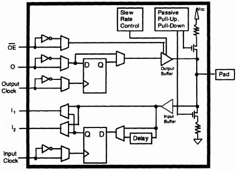
Figure 8–12. Block diagram of the XC4000 Input/Output block (IOB).
A master three-state control, when active, places all the I/O blocks in a high-impedance mode. Such a function often is useful during board test operations, or to put the FPGA in a passive, low-power state in battery-driven applications.
Programmable Interconnect All internal connections are composed of metal segments with programmable switching points provided to implement the desired routing. A rich amount and variety of routing resources was chosen to allow efficient automated routing. Routing is scaled to the size of the array, that is, the number of routing channels increases with array size. The CLB’s inputs and outputs are distributed on all four sides of the block, for added routing flexibility. In general, the entire architecture is more symmetric and regular than the previous generations, and is more suited to well-established placement and routing algorithms developed for conventional mask-programmed gate array design.
The routing scheme was designed to minimize the resistance and capacitance of the average routing path, resulting in significant performance improvements. There are three main types of interconnect, characterized by the relative length of their segments: single-length lines, double-length lines, and long lines. The single-length lines are a grid of horizontal and vertical lines that intersect at a “Switch Matrix” between each block. The number of possible connections through the Switch Matrix has been streamlined compared to the previous generations of FPGA architectures, in order to reduce capacitive loading to minimize routing delays and increase performance. However, a much richer set of connections between the single-length lines and the CLB’s inputs and outputs more than compensate for this reduction in Switch Matrix options, resulting in overall increased “routability.” Double-length lines, as implied by their name, run past two CLBs before entering a Switch Matrix, for efficient implementation of intermediate length interconnections. Long lines run the entire length or width of the array, and are intended for high fan-out control signals. Each vertical long line has a programmable “splitter switch” at its center, allowing the long line to be used as two independent routing channels that each run half the height of the array. Automated routing software uses this hierarchy of routing resources to achieve an efficient implementation of a given application.
Eight low-skew global buffers are provided for distributing clocks and other high fan-out control signals throughout the device. Overall skew on these global nets is less than 2 ns, even in the largest devices. An internally-generated clock signal also is available to the user.
Three-State Buffers and Edge Decoders Associated with each CLB in the array are a pair of three-state buffers that can be used to drive signals onto the nearest horizontal long lines above and below the block. Additional three-state buffers are located near each I/O Block along the right and left edges of the array. These buffers can be used to implement multiplexed or bi-directional busses on the horizontal long lines. Programmable pull-up resistors attached to these long lines facilitate their use for wide wired-AND logic functions.
Fast decoding is a requirement in many high-speed microprocessor systems. When the width of the decoding function exceeds the fan-in of the logic block in the FPGA, the use of multiple levels of logic blocks can result in unacceptable performance delays. The XC4000 architecture addresses this need with 16 dedicated “edge decoders,” four along each edge of the chip. These “wired-AND” circuits accept inputs from nearby IOBs and CLBs; for example, each edge decoder in the XC4010 accepts up to 40 inputs from adjacent IOBs and 20 inputs from on-chip, and generates a decoded output in 11 ns.
The XC4000 Family The XC4000 family is at the time of writing the broadest available family of FPGAs, ranging from the 2,000-gate XC4002A to the 25,000-gate XC4025 (Table 8–1). For applications requiring many I/O pins but modest logic capacity, the XC4003H and XC4005H feature about twice as many I/O blocks as the base family members; these devices do not include registers in the I/O Blocks. This breadth of product offerings allows designers to select the FPGA device that is most cost-effective for the target application.