Chapter 33
Making Circuit Boards
You’ve built your robot, and it’s ready to rumble. You’ve tested its control electronics on a solderless breadboard, and everything’s a go. But now you want to commit the breadboard electronics to a permanent circuit board. Your bot will be more ruggedized, and it’ll withstand your nephew’s pawing (don’t blame him for loving robots as much as you do!).
When it comes to making circuit boards, you’ve got plenty of choices. In this chapter you’ll learn about the most popular (and most affordable) circuit-board-making techniques. All are suitable for the amateur and educational robot builder, though those involving dangerous chemicals are ill-advised for children, even with adult supervision.
Overview of Your Primary Circuit Board Options
Before getting down to the nitty-gritty here’s a quick overview of your best options:
![]() Solder breadboards. These mimic the solderless breadboards you read about in Chapter 32, but these are made for permanent soldering.
Solder breadboards. These mimic the solderless breadboards you read about in Chapter 32, but these are made for permanent soldering.
![]() Unplated perforated boards. Old-fashioned but still useful for very simple circuits, these are boards with holes already drilled in them. You wire up components directly.
Unplated perforated boards. Old-fashioned but still useful for very simple circuits, these are boards with holes already drilled in them. You wire up components directly.
![]() Plated stripboards. Same idea as above, but these are plated in different grid styles to avoid wiring directly to component leads. Easy to work with and cheap. Lots of variety.
Plated stripboards. Same idea as above, but these are plated in different grid styles to avoid wiring directly to component leads. Easy to work with and cheap. Lots of variety.
![]() Quick-turn printed circuit boards. Design a printed circuit board (PCB) on your computer, then send it out for manufacturing. Less expensive than you may think.
Quick-turn printed circuit boards. Design a printed circuit board (PCB) on your computer, then send it out for manufacturing. Less expensive than you may think.
![]() Home-etched PCBs. Using a strong chemical, you can etch the pattern of your own PCB onto a copper-plated board. Time-consuming and messy, but can be a good learning experience.
Home-etched PCBs. Using a strong chemical, you can etch the pattern of your own PCB onto a copper-plated board. Time-consuming and messy, but can be a good learning experience.
![]() Custom prototyping boards. Some components with “rock star” status (most notably, microcontrollers like the PICAXE, AVR, and PICMicro) have various custom prototyping boards available for them. Take your pick.
Custom prototyping boards. Some components with “rock star” status (most notably, microcontrollers like the PICAXE, AVR, and PICMicro) have various custom prototyping boards available for them. Take your pick.
![]() Wire wrapping. Semipermanent construction using very thin wire between components. You can undo the wires to make changes.
Wire wrapping. Semipermanent construction using very thin wire between components. You can undo the wires to make changes.
There are other methods that I’ll be skipping here. Many are out of date, are specific to one manufacturer, require hard-to-find parts, or may require special tools.
Clean It First!
Circuit boards use a thin layer of copper to form traces, the wires of the circuit. Copper can oxidize and get dirty over time, both of which can lead to a poor solder joint. No matter which circuit-board-making method you use, prior to any soldering be sure to thoroughly clean the board using warm water and ordinary kitchen cleansing powder. You can scrub the board using your fingers, a folded-up paper towel, or a nonmetallic scouring pad.
After cleaning, rinse all of the cleanser off the board. Pat it dry with a paper towel, then let it air-dry—it takes a couple of minutes. For a superclean board, wet a cotton ball with household isopropyl alcohol and give the metal a final wipedown. Allow all of the alcohol to evaporate.
Making Permanent Circuits on Solder Breadboards
Akin to the solderless breadboard is the solder breadboard, where you can make permanent any design you create on a solderless breadboard.
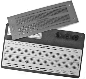
Figure 33-1 A solderless breadboard and a companion solderboard. Test your circuits on the solderless breadboard, and once the design is finished, debugged, and working, transfer the components to the solderboard following the same arrangement.
The solderboard comes pre-etched with 550 tie points. Circuits may be designed on a solderless breadboard, then transferred to the solder board when you’re sure everything is working to your liking. Simply solder the components into place following the same design you used on the solderless board. Use jumper wires to connect components that can’t be directly tied together. Figure 33-1 shows both a solderless and a solder breadboard.
Small circuits take up only a portion of the solder breadboard. You can cut off the extra using a hacksaw or razor saw. (But beware of the “sawdust” from these boards; it’s not healthy for you, so don’t inhale or ingest any of it.) Leave space in the corners of the board to drill new mounting holes, so that you can secure the board inside whatever enclosure you are using. Alternatively, you can secure the board to a frame or inside an enclosure using double-sided foam tape.
If you’re constructing small circuits, one solderboard will last for several projects. In time, you’ll learn how to conserve space to make good use of the real estate on a solderboard.
Using Point-to-Point Perforated Board Construction
An alternative to the solder breadboard is point-to-point perforated (or “perf”) circuit board construction. This technique refers to mounting the components on a predrilled board and connecting the leads together directly with solder. Perf boards are basically just blank pieces of phenolic or other plastic, with holes drilled every 0.1″. This is the correct spacing for standard integrated circuits, and it works well for other components.
For robot electronics, point-to-point perf board construction is best used—if at all—for very simple circuits containing just a few components. You use the board as a kind of structure for the electronic parts.
BUILDING A CIRCUIT ON A PERF BOARD
Figure 33-2 shows the concept behind using a perf board—again, it’s merely a board with holes already drilled into it. Basic construction goes like this:
1. Cut the board to the size you’ll need for the circuit. You’ll need to estimate the amount of board space.
2. Insert one component at a time through the holes of the perf board. Bend the leads on the opposite side to keep the component from falling out.
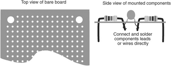
Figure 33-2 When using a perforated (perf) board, you directly connect components together or solder component leads with insulated jumper wires.
3. For components that are right next to one another, wrap leads that connect. One or two turns is enough.
4. For connecting components that are more than an inch or two from one another, use 30-gauge wire meant for wire wrapping (see the section on wire wrapping, later in the chapter), strip off about 1/2″ of the insulation from the end of the wire, and hook it around the component lead.
5. Use a soldering pencil to flow some solder to the wires.
6. Repeat until all the components are mounted and wired together.
7. Trim off any excess wire lengths to avoid short circuits. Double-check your work.

Perf board wiring is often referred to as bird’s-nest construction—you can guess why. For circuits using more than a couple of components, use a copper layout board, detailed next. Since circuits on point-to-point perf boards are delicate, mount them on your robot using one or two small fasteners or a cable tie. Avoid having the board just flop around loose.
ALTERNATIVES TO PERF BOARD MOUNTING
A variation on the theme of point-to-point wiring on a perf board is to simply do away with the perf board. Over the years, a variety of techniques have been developed; here are some of them:
![]() Dead bug wiring is sometimes used with a single IC connecting to just a few components. It’s called “dead bug” because when the chip is turned upside down, and things are soldered to its pins, it looks a bit like a little, black, dead bug. When soldering on resistors, capacitors, and similar components, cut the lead to length, then bend the end to make a U shape. Solder the U directly to the IC pin.
Dead bug wiring is sometimes used with a single IC connecting to just a few components. It’s called “dead bug” because when the chip is turned upside down, and things are soldered to its pins, it looks a bit like a little, black, dead bug. When soldering on resistors, capacitors, and similar components, cut the lead to length, then bend the end to make a U shape. Solder the U directly to the IC pin.
![]() Wire wrap sockets have extra-long pins for attaching to wires. The IC itself plugs into the socket after construction is complete. As with dead bug wiring, you can form fairly strong solder joints by bending the end of the component lead into a U and hooking it around the socket pin.
Wire wrap sockets have extra-long pins for attaching to wires. The IC itself plugs into the socket after construction is complete. As with dead bug wiring, you can form fairly strong solder joints by bending the end of the component lead into a U and hooking it around the socket pin.
![]() Lead-to-lead construction is suitable when you’re soldering the leads of one discrete component to another—for example, a resistor to an LED. Prepare the leads of both components by cutting them to the desired length, then form small hooks to make a good mechanical joint. Solder the two together.
Lead-to-lead construction is suitable when you’re soldering the leads of one discrete component to another—for example, a resistor to an LED. Prepare the leads of both components by cutting them to the desired length, then form small hooks to make a good mechanical joint. Solder the two together.
Using Predrilled Stripboards
A stripboard has holes drilled in it, just like a perforated board. But on at least one side of the board is a series of copper metallic pads and/or strips that run through the center of the holes. These boards come in a variety of sizes and styles. All are designed for use with ICs and other modern-day electronic components. One application of the stripboard is circuit construction using wire wrapping, as detailed later in this chapter. But many circuits can be soldered directly onto the board.
Choose the style of grid board depending on the type of circuit you are building. Figure 33-3 shows a selection of basic grid layouts. Variations include:
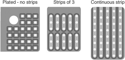
Figure 33-3 Example grid layouts for perforated stripboard. Select the layout that best matches the circuit you’re building and your construction preferences.
Plated holes without strips: These are used like perforated boards, previously described, but you can solder component leads to the copper plating around the holes. You then complete the board by attaching wires to the component leads.
Continuous strips that run the length of the board: To make a circuit, solder in components and wires, then use a sharp knife (or a specialty spot face cutting tool) to break the strip after all the connections are made for that particular part of the circuit.
Strips in groups of three to five holes: Rather than have you cut a long strip into smaller segments, these boards have done it for you. Each segment spans from three to five holes (sometimes more). Some boards have additional strips running perpendicular to the segments; these are common busses for easy connection to positive and negative terminals from the power supply.
Personally, I prefer boards with the three-hole segment plan. Components are tied together using three-point contacts. If you need to connect more components to a single point, you can link multiple segments together by bridging them with a piece of wire. Those boards with the extra strips for positive and negative terminals are ideal for circuits that use many integrated circuits, as it simplifies connection to power. The interleaving of the power supply rails also helps reduce electrical noise.
Always use either the plated copper segments to bridge components together or else a length of bare wire. Avoid the temptation of using a big blob of solder to bridge segments together.
Creating Electronic Circuit Boards with PCB CAD
Thinking about making your own printed circuit boards? Here’s one way: start by laying out your circuit on paper, then transferring that as a photoresist to a piece of copper-cladded fiberglass sheet. You then mix up a nasty (and toxic) soup of ferric chloride and dip the board into the liquid for 20 minutes, hoping none of it gets on your clothes. You then painstakingly drill all the holes and—voila!—your printed circuit board (PCB) is ready for soldering.
Or you could just prepare the board using free design software, then click a Send button. In a few days you get back a professionally produced single- or double-sided PCB through the mail. For just a few dollars more, your custom PCB board can even include silkscreen printing, where all the parts are indicated in white ink.
Automated printed circuit board manufacturing is a kind of quick-turn prototyping. In Chapter 15, “Drafting Bots with Computer-Aided Design,” you learned how quick-turn prototyping can build mechanical parts out of metal or plastic. When the concept is applied to circuit boards, you get a two-dimensional PCB.
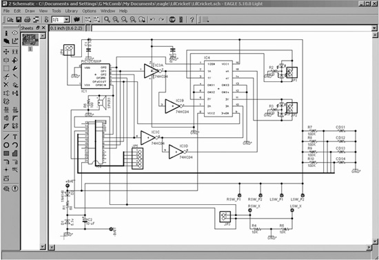
Figure 33-4 Schematic for L’il Cricket, drawn and executed in CadSoft Eagle.
Many PCB service bureaus (companies that make PCBs for you) rely on their own proprietary electronic computer-aided design (ECAD) software to lay out the board. If the service bureau doesn’t offer an ECAD program you can use, you’ll need to get one compatible with their system. The free version of CadSoft’s Eagle program is one popular option; it’s limited to laying out boards measuring up to 4″ by 3.2″. If you need to build larger PCBs, opt for the full version of Eagle.
Figure 33-4 shows the schematic for L’il Cricket, a buglike robot designed in Eagle. The robot measures about 5″ × 3″, where its PCB is also its body.
Figure 33-5 shows a completed PCB layout. I placed the components where I wanted them to be, and Eagle autorouted (figured things out by itself) the connecting points between everything, based on the schematic that I previously prepared. This is a two-sided board, so there are copper traces connecting components on both the top and bottom. Note that the PCB view also includes a silkscreen layer, which contains the outlines and labels of the parts. Read more about this feature in the following section.
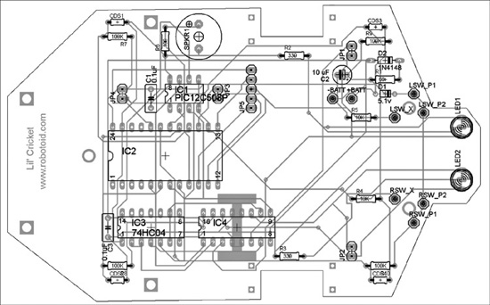
Figure 33-5 PCB layout for L’il Cricket, made by Eagle. The layout is ready to be sent to a PCB service bureau for production. To create the layout, the components were placed where I wanted them, and then Eagle autorouted the connections following the schematic I had already prepared.
Whether you use Eagle or some other software, here is the basic process for designing and making your printed circuit board:
1. Create a schematic of your circuit. The schematic uses symbols for all electronic parts and lines to indicate how everything is connected together.
2. Create the PCB layout by dragging the outlines of your parts onto a template of the size of board you want.
3. Convert the schematic and the PCB layout. Finish the PCB design by linking components that need to be connected.
4. If you are having a service produce the board, order the board by submitting it. Payment is collected up front. Most services will prepare two or three boards for the base price.
PRINTED CIRCUIT BOARD DETAILS
Following are concepts you should know about when making printed circuit boards:
Pads, traces: PCBs are composed of pads and traces. The metal leads of the components are soldered to pads, and the pads are connected together via traces. The traces are the interconnecting wires of a PCB.
One or two sides: All printed circuit boards have two sides, but you may elect to have pads and traces on one side only. It’s a little cheaper that way.
Layers: Each side of the PCB can be separated into individual layers. The layers are insulated from one another by a protective film, so that the pads and traces in one layer don’t short-circuit into those of another layer. Your quick-turn PCB may have two, four, six, even eight layers. The more layers, the more expensive it is.
Soldermask: If you choose to order it as an option, a soldermask applies an insulating lacquer over your board that covers everything except the pads to which components are to be soldered.
Silkscreening: Another option is the silkscreen legend, which marks where the components go. You can include the outline shapes of the components, component values, part number references, even limericks. It’s completely up to you.
Producing Arduino-Specific Boards with Fritzing
Fritzing (available at www.fritzing.org) is a nifty, free ECAD program designed for creating printed circuit boards. What sets it apart is that it is designed from the ground up to support the open-source Arduino, one of the key microcontrollers used in projects throughout this book.
By connecting wires on a virtual solderless breadboard, your circuit designs are automatically converted to schematics and printed circuit board layouts. These layouts are meant to be Arduino shields, circuit boards that attach on top of the Arduino and extend its functionality. (The Arduino and shields are detailed in Chapter 37, “Using the Arduino.”)
Figure 33-6 shows one of the example projects that come with the Fritzing software, a stepper motor experimenter board. Simply by clicking tab buttons inside the Fritzing program, you can view the circuit as a schematic (see Figure 33-7) and even as a Arduino shield PCB.
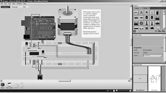
Figure 33-6 Virtual breadboard view of an Arduino project created in the Fritzing ECAD software. This is one of the projects that comes with the free Fritzing software.
You can export the PCB layout as an etchable PDF, then print the PDF using special film that can then be transferred to a bare copper-clad circuit board. This involves immersing the prepared board in a caustic chemical to remove the extra copper, and then drilling out holes for the components.
Other board-making options using Fritzing include exporting the design to an Eagle file for use with the CadSoft Eagle PCB software, mentioned earlier. Or you can convert the layout to a series of Gerber files that contain all the information that an automated PCB quick-turn service can use to prepare your board. The files generated by Fritzing specify the actual pattern layout, soldermask, silkscreen, and hole sizes that are to be used.
Fritzing will even generate a “bill of materials” (BOM) file for you, listing all the components used in the project. The BOM file is stored as text, but it’s in Unicode format. Microsoft Word can read a Unicode-encoded file, but Windows Notepad and many other text-only editors won’t know what to make of it. It’ll just look like gibberish.
On the Web: Etching Your Own Printed Circuit Board
So far, I’ve talked about designing a PCB using a layout program, then shipping the files off to a service that makes the board for you. By far, this is the most convenient approach; but it’s also the more expensive route. It’s cheaper (in terms of money) if you make the board yourself.
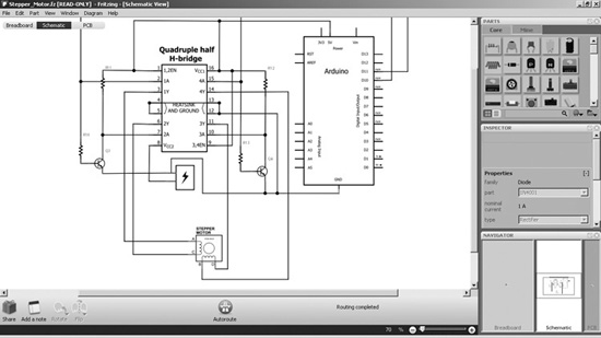
Figure 33-7 From the breadboard view, Fritzing can automatically generate a schematic diagram. You can adjust the drawing to fine-tune it.
The process of making your own printed circuit boards is not complex or even difficult, but it is time consuming, and it does involve using some nasty chemicals that cause stains on clothing and burns on skin. With the advent of low-cost PCB service bureaus, making your own circuit boards is something of a dying artform. If you’re interested in the techniques used to make your own printed circuit boards, check out the bonus tutorials about it on the RBB Online Support site (see Appendix A).
Using Custom Prototyping Boards
The popularity of several brands of microcontrollers has spawned a kind of cottage industry in prototyping (or proto) boards custom-made for them. Proto boards are empty PCBs with layouts and predrilled holes to accommodate a wide variety of projects.
You start by soldering the microcontroller into its spot (better yet, use an IC socket, then plug the controller into the socket), then complete the board by adding other components. Many prototyping boards have a reserved section for general experimenting, where you can add your own circuits to the basic one already there. Some proto boards are even made with mini solderless breadboards stuck to them.
Some proto boards already have the microcontroller soldered to them. In this case, the controller may be in a more compact format than the typical dual in-line package (DIP) you’re most familiar with. This makes using the board very convenient, as the controller is already built in.
The disadvantage is that if the MCU is not in a socket, any damage to the chip means the entire prototype board is a loss. My preference is to use a prototyping board that accepts the standard DIP IC packages, and then use sockets to allow easy swapping of controllers.
Making Semipermanent Circuits with Wire Wrapping
With wire wrapping there’s no soldering (or at least only very little); instead, plug a special socket into a perforated board, and then wrap thin wire around the pins of the socket using a special tool. The advantage of wire wrapping is that it’s relatively easy to make changes. Just unwrap the wire and reroute to another post.
Wire wrapping is commonly used in IC-intensive circuits. The construction technique doesn’t promote fast results, but because soldering is usually not involved it’s a safer bet for kids interested in learning electronics. And, of course, mistakes are easier to correct than when using solder construction.
HOW WIRE WRAPPING WORKS
To wire wrap, first mount a wire wrapping socket into the perforated board. Sockets are available for all the common sizes of DIP-style ICs. I prefer to use a perf board with copper pads around the holes so that I can apply a tiny bit of solder to at least one of the pins of the socket. This keeps the socket from falling out while I’m working on the board.
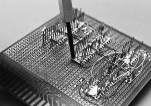
Figure 33-8 Wire wrapping creates circuits by literally wrapping wire around metal posts.
Wire wrapping sockets use extra-long square-shaped pins (also called posts) that can accommodate up to about five wrapped wires. Using a special tool, as shown in Figure 33-8, each wire is wrapped around the pin like figures on a totem pole. Once the wire is wrapped about a half-dozen times around the pin, the connection is as solid and secure as a soldered joint.
CHOOSING A WIRE WRAPPING TOOL
You need a special tool for wire wrapping. A manual wire wrapping tool is shown in Figure 33-8. To use it, you insert one end of the stripped wire into a slot in the tool, then place the tool over a square-shaped wrapping post. Give the tool 5 to 10 twirls, and the connection is complete. The edges of the post keep the wire anchored in place. To remove the wire, use the other end of the tool and undo the wrapping.
Other tools are motorized, and some automatically strip the wire for you, which frees you of this time-consuming task (or the need to purchase the more expensive prestripped wire). I recommend that you start with a basic manual tool. You can graduate to other tools if you find wire wrapping suits you.
Successful wire wrapping takes practice. Before you build your first circuit using wire wrapping techniques, try your hand on a scrap socket and board. Visually inspect the wrapped connections and look for loose coils, broken wires, and excessive uninsulated wire at the base of the post. Most wire wrap tools are designed so one end is used for wrapping wire and the other end for unwrapping. Undo a connection by inverting the tool, and try again.
WIRE: SPOOLS OR PRECUT
You can purchase 30-gauge wire for wire wrapping by the full spool, but unless you’re going into full-fledged production, a far easier method is to get precut wire in a couple of different lengths—2″ and 4″ lengths make for a good start (that’s the length of the wire not counting the bare ends).
When using spools, you must cut the wire to length, then strip off the insulation using the stripper attached to the wrapping tool. A stripper for regular wire does a poor job because the insulation on wire wrapping wire is extra tough. These steps greatly add to the time it takes to make a single wire wrapped joint.
When you use the precut or prestripped packages, the work is already done for you. Buy a selection of different lengths, and always try to use the shortest length possible. Precut and prestripped can be expensive ($5 or more for a canister of 200 pieces), but it will save you a great deal of time and effort.
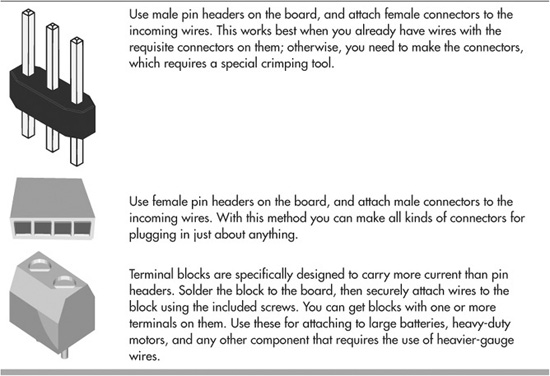
Effective Use of Plug-in Headers
Nothing in life is certain but death, taxes, and robot circuit boards with too many wires on them. You can take the easy route and just solder all the wires directly to the robot’s circuit board, but a better approach is to take a cue from automobile manufacturers: use lots and lots of connectors.
These three methods are the most popular: