
CMOS THz Wireline Communication 299
14.2 Surface Plasmon Polariton T-Line
The surface plasmon po lariton (SPP) propagating at the flat interface be-
tween a real metal and a dielectric are naturally 2D electromagnetic waves.
Confinement of EM wave is realize d since the propagation constant is greater
than the wave vector k within the dielectric, resulting in evanescent decay
on both sides of the interface. Essentially, because the SPP dispersion curve
lies to the right of the light line o f the dielectric (given by ω = ck ) [302],
among optical applications the SPPs excited by 3D light beams is impossi-
ble unless sp ecial techniques for phase-matching are utilized. Various optical
techniques have been proposed to fulfill phase matching, inc luding grating
coupling and e xcitation with highly focused beams. Normally, for geometries
exhibiting strong field-localization below the diffraction limit, the overlap be-
tween the excitation beam and the coupled SPP mode is small, leading to low
excitation efficiency.
While those optical excitation schemes are suitable for the development of
SPP propagation and functional plasmonic structur es, in practice the SPPs
used in the design o f integrated circuits will normally require high conver-
sion efficiency (and hence large-bandwidth) coupling schemes. In order to
make full use of the benefit of wide bandwidth in o ptics designs, the plas-
monic structures should allow for efficient matching with conventional optical
waveguides or fib ers, which would be used in such a scenario to guide energy
over long distance onto plasmon transmission lines and cavities with broad
bandwidth. However, in on-chip electronic communication, the on-chip inter-
connect is generally connected to CMOS transistors or other passive devices
which in fact have narrower bandwidth than optical devices. At the s ame
time, the converter with exponentially grading CPW reported in Ref [294], is
difficult to be integrated on chip. As such, it is more impo rtant to first in-
vestigate the impedance matching and resulting return loss for the realiz ation
of the on-chip SPP T-line. Normally, there ar e two major lossy mechanisms
contributing to the guiding loss of SPP T-lines: the return loss and the inser-
tion loss (or transmission loss ). While the insertion loss can be improved over
other traditional T- line s tructures due to the confinement of EM energy, the
return loss begins to dominate as long as the periodical array decouples the
incident beam into the propagating SPPs. To understand how the mismatch
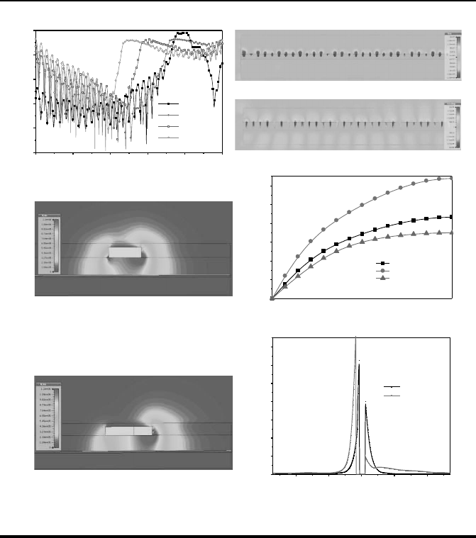
affects the excitation, Figure 14.2(a) shows the input reflection coefficient of
the designed on-chip SPP T-line as a function of groove depth h. A plane
TEM wave is injected from one end of the structure while the other end is
terminated. As observed, the designed structure cannot maintain highly ef-
ficient coupling from 3–6 THz, which c onfirms the limited bandwidth of the
input matching. On the other hand, the SPP coupling efficiency trades off
the c onfinement of the surface wave. In general, the tight co nfinement can be
achieved by mer ely increasing the groove depth for this structure, which will
be discussed later. However, this does not nece ssarily bring about the same
amount of improvement if the coupling efficie nc y is taken into account: the
300 Design of CMOS Millimeter-Wave and Terahertz Integrated Circuits
1 2 3 4 5 6
-50
-40
-30
-20
-10
0
S11 (dB)
Frequency (THz)
h=4um
h=7um
h=10um
h=13um
-100 -50 0 50 100
0.0
2.0x10
5
4.0x10
5
6.0x10
5
8.0x10
5
1.0x10
6
1.2x10
6
1.4x10
6
|Ey|
Curve Length / um
h=6um
h=12um
(a)
(b)
(c)
(d)
(e)
(f)
0 20 40 60 80 100 120 140 160 180
0.0
0.2
0.4
0.6
0.8
1.0
1.2
Frequency (THz)
Theta
d=h=30um
d=h=20um
d=h=40um
(g)
Figure 14.2: (a) Simulated input reflection coefficient of the designed
on-chip SPP T-line for different groove depth h with d = 15 µm,
a = 2.4 µm, w = 5 µm. (b– c) The simulated amplitude of E-field
distribution of the d esigned SPP T-line (a: h = 6 µm, b: h = 12
µm) evaluated at the xy plane using the CMOS process. (d–e) E-field
distribution on the cross-section of the corrugated m etal strip: h = 6
µm, d: h = 12 µm) at yz plane, also at 3 THz, and (f) the simulated
dispersion diagram with different periodic pitch d and groove depth
h ranged from 20 µm to 40 µm. (g) E-field enhancement along the
vertical cut for h = 6 µm and h = 12 µm, respectively.
higher the confinement, the lower the bandwidth of efficient coupling. Physi-
cally, due to the momentum mismatch at the interface, only a small fraction
of the incident TEM wave can be converted to SPPs mode and coupled to the
periodical structure, leading to strong reflection of incident wave and energy

CMOS THz Wireline Communication 301
(a)
(b)
Figure 14.3: (a) The simulated amplitude of E-field distribution of
the conventional transmiss ion line evaluated at the xy plane using
the same process, and (b) E-field distribution on the cross-section of
the corrugated metal strip (yz plane) also at 3 THz. The width of
T-line is 11 µm with wideband impedance m atching up to above 3
THz.
loss. As a c onclusion, the loss of SPP T-line cannot be reduce d by rendering
the structure when only to obtain a tight c onfinement.
Recall that for a co mpact SPP T-line struc ture, the retur n loss is pretty
high at several terahertz due to the low coupling efficiency of the incident beam
to propagating SPPs. It appears lower than -10 dB at a round 1 THz, along
with the penalty of weaker field-localization below the diffraction limit. This
does not necessarily mean that the coupling efficiency becomes more effective
at lower frequencies. In this case, the dispersion diagram of propagating SPPs
starts to bend with respect to the light line but the bending de gree is lower
than that of strong field-localization, which indicates that part of EM energy
maintains their polarization property when being injected into the s tructure.
In fact, the co nfinement of surface mode can be evaluated through the disper-
sion diagram [29 4, 169], and the SPP T-line behaves in purely propa gating
surface mode only if it operates close to the plasma asymptotic frequency
(several terahertz for the dimension given in Figure 14.2(a )), which is difficult
for CMO S on-chip transmissio n s inc e the physical dimension becomes pretty
large. This scenario is apparently different from the case of board-level imple-
mentation in the microwave region [294, 169, 295, 296, 297, 298], in which the
substrate can be either made by an insulation layer or even removed. Instead,

302 Design of CMOS Millimeter-Wave and Terahertz Integrated Circuits
100 200 300 400 500 600 700 800
-45
-40
-35
-30
-25
-20
-15
-10
-5
Return Loss (dB)
Frequency (GHz)
1mm
3mm
Ground
Ground
y
x
a
d
h
(a)
(b) (c)
Figure 14.4: (a) The layout of SPP T-line including EM wave to
surface wave (or vice versa) converter and with M1 as ground, (b)
converter design and conceptual E-field distribution , and (c) the sim-
ulated result of reflection coefficient (S
11
).
in the following, we investigate the SP P property by desig ning a c ompact
SPP T-line str uc ture operating at frequencies that are away from the plasma
asymptotic frequency region.
The CMOS-based SPP T-line structure is designed as s hown in Figure
14.1. The period pitch d is chosen to be 15 µm which is far less than the op-
eration wavelength (λ = 1 mm), and the line width w is 5 µm. Note that the
conventional microstrip line with w = 5 µm has a characteristic impedance
of 50 Ω fro m 10 GHz to 3 THz in this process. As the line is s tructured, the
SPP modes are generated, which can be co nfirmed by the full-wave ne ar-field
simulation using FDTD with the boundary condition set as open to simulate
the real spac e. The boundaries are at a large dista nc e from the metal struc-
ture to avoid significant reflections. With the surface mode confined by the
corrugated strip, we are now in a position to evaluate the E -field distribution
of the guiding structur e.
Figures 14.2(b) and (c) illustrate the simulated E-fields (E
x
components)
evaluated a t the top of corrugated strips with different corrugation de pth at
3 THz. The gray-scale from highest to lowest density indicates the tight con-
finement of EM wave within the comb-shaped metal strip. In this experiment,
CMOS THz Wireline Communication 303
instead of defining a monopole excitation, the TEM wave is injected from one
terminal of this periodical T-line with the other terminal loaded with 50Ω
impedances. Due to a non-perfect transition from the TEM wave to the sur-
face wave at the injection interface, the excited surface mode is no t completely
restricted within the groove. However, one can still observe that part of the
EM field is strongly localized within the co mb-shaped metal structure and de-
cays at the metal/dielectric interface. We observe that the sur face EM waves
are tightly confined and propagate a long the SPP T-line with small losses at
3 THz as well. In addition, the confinement of the surface mode can be effec-
tively improved by solely incr easing the gr oove depth, which can be further
confirmed by the observation of corresponding E-field distribution shown in
Figures 14.2(d) and (e) a t the yz plane, in compliance with the findings in
the microwave region using the similar structure [294, 169]. A ground plane
realized by the bottom copper metal is implemented to ensure that the E-field
is mainly restricted between the two conductors. Without the ground, a great
portion of energy will be absorbed by the lossy substrate, and the resulting
confinement by the de signed structure becomes less effective. Again, the dis-
persion diagram is re-simulated with the consideration of ground. It shows
that the asy mptotic frequency is still clearly bending away from the light line
except that it slightly increase s. The dispersion relation is further examined
by varying the groove depth h as shown in Figure 1 4.2(f).
Clearly, the asymptotic freque nc y decrease s with deepe r grooves, consis-
tent with the cas e without ground beneath the SPP T-line. When both the
periodical pitch d and groove depth h are equal to 40 µm, the asymptotic fre-
quency is down to approximately 0.6 THz, presenting stronger confinement in
the sub-THz region. As such, the ground plane inherently has negligible influ-
ence on the SP P property while it helps to further reduce radiation loss. The
details of confinement can be clearly observed from E-field enhancement in the
cross-sections perpendicular to the strips, as illustrated in Figure 14.2(g). The
field clearly decays exponentially along the or thogonally lateral y direction,
illustrating the typical feature of SPP mode. In summary, the above study
reveals the feasibility of confining surface mode with the periodical groove
structured T-line in the CMOS proces s.
In contrast to TM polarization in the SPP T-line, the conventional trans-
mission line propagates TEM mode a long the structure. As shown in Figure
14.3(a), the current intensity of the microstrip line tends to crowd on the
metal surfac e. Note that in such a scenario the effective metal resistance will
be incr eased and in return degrades the signal transmission. Given that the
E-field is dominating near the metal surface, more energy would be radiated
out in the fo rm of radiation loss and crosstalk to adjacent conductors. Even
though most of the E -field is restricted to the metal surfaces between T-line
and ground as illustrated in E-field distribution at the yz plane, as shown
in Figure 14.3(b), the radiation outside of T-line remains strong, lea ding to
more e ne rgy penetration into the dielectric medium and hence results in larger
radiation loss. Similarly, despite the fact that ground plane has considerable
..................Content has been hidden....................
You can't read the all page of ebook, please click here login for view all page.