

214 Design of CMOS Millimeter-Wave and Terahertz Integrated Circuits
Figure 9.1: (a) Stacked SRR un it-cell designed by metal layers of M7
and M6; (b) S21 simulation results with different stacking methods.
oscillator s based on metamaterial r esonators have bee n designed in 65-nm
CMOS (STM 7-metal-layer). The first one is operated at 76 GHz using the
differential T-line loaded with SRR (DTL-SRR), and the second one is op-
erated at 96 GHz using the differential T -line loaded with SRR (DTL-SRR).
Note that the design of slow-wave shielding is implemented for both MMIC
oscillator s with loss reduction. The slow-wave shielding strips are designed
by the bottom metal layer M1 with both width and pitch of 1 µm. The two
MMIC oscillators are designed and verified with Agilent ADS Momentum for
EM simulation and Cadence Spectre for oscillator circuit simulation.
9.2 Differential TL-SRR Resonator
9.2.1 Stacked SRR Layout
The on-chip SRR can be implemented in a stacked fashion with on-chip multi-
layer interconnect [84]. As shown in Figure 9.1(a), one SRR unit-cell is real-
ized by the top two metal layers stacked alternatively, considering a trade-off
among resonant frequency, area and los s. When its size is fixed, S21 of TL-
SRR with differ ent stacked layers is shown in Figure 9.1 (b). It is found that
more stacked layers result in lower resonant frequency, but suffer from lower
Q at the same time. With the inc reased resonant fr equency, TL-SRR reveals a
steeper and higher rejection property, which means a higher Q. Thus T L -SRR
shows the potential application for on-chip MMIC designs.
Figure 9.2(a) shows a differential T-line with stacked on-chip SRR (DTL-
SRR) in the CMOS proc ess, o f which the cross- section is illustrated in Figure
9.2(c). The two loaded SRR unit-cells are excited by the axial mag ne tic field
generated by the host T- line . It has the following advantages in Q impr ove-
ment. Firstly, as the SRR-load is metamaterial with stop-band property, it
Resonator 215
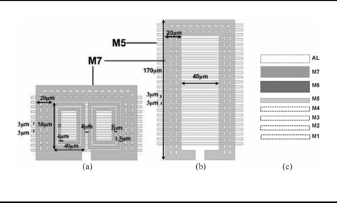
Figure 9.2 : Geometries of resonators with slow-wave shielding: (a) dif-
ferential T-line loaded with stacked SRR, (b) T-line based standing-
wave resonator, and (c) cross-section of BEOL.
results in large impedance with the open circuit condition formed. Thus EM
energy can be perfectly reflected in the host T-line. Secondly, the differential
design provides local ground to reduce EM loss and enhance the EM- energy
coupling. For example, the magnetic field ge ne rated by the differential T-line
is equidire ctional and superimposed when applied to the two SRR unit-ce lls.
Thus a str onger coupling between T-line and SRR is achieved with larger
mutual ca pacitance and mutual inductance, which can store more EM-energy
with less EM-energy leakage into the substrate. Due to the stronger EM cou-
pling, the DTL-SRR needs fewer SRR unit-cells than STL-SRR when the
same rejection property is achieved. This makes the DTL-SRR achieve higher
area efficiency as well. To strengthen the coupling between T-line and SRRs,
a shortest distance (or gap) b etween SRRs and T- line is selected with the
consideratio n of the process limitation (1.5 µm in STM 65nm CMOS). Lastly,
floating metal shie lding is also employed in this design to further reduce the
substrate loss.
9.2.2 Comparison with Single-Ended TL -SRR
Resonator
In the following, detailed analys is for the enhancement of Q factor is shown
with co mparison between the DTL-SRR and STL-SRR. Assuming both ter-
minals of an SRR unit-cell observe the same characteristic impedance (Z
0
).
The reflection coefficient can be estimated at the position TL-SRR unit cell
216 Design of CMOS Millimeter-Wave and Terahertz Integrated Circuits
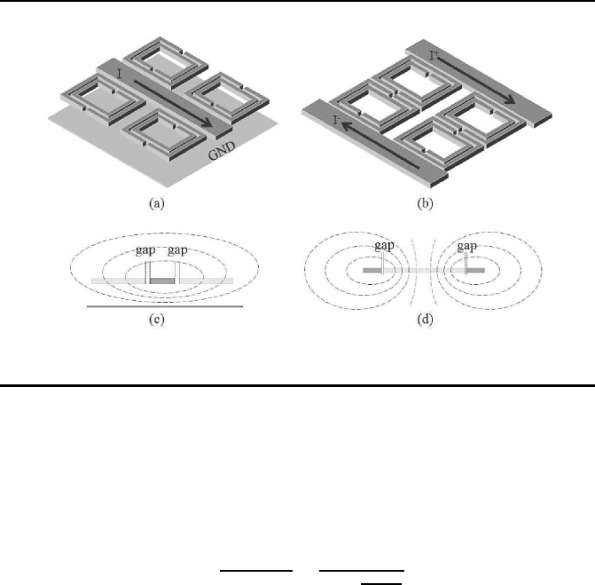
Figure 9.3: T-line-based SRR excitation: (a) s ingle-ended approach,
(b) differential approach, (c) magnetic field distribution of single-
ended approach, and (d) magnetic field distribution of differential
approach.
by
Γ =
R
′
s
R
′
s
+ 2Z
0
=
k
2
k
2
+
2Z
0
L
s
R
s
L
. (9.1)
One can have two observations fro m (9.1). Firstly, if the Q factor of SRR is
sufficiently high that k
2
>> 2Z
0
L
s
/R
s
L, Γ is a pproaching unity, which means
a perfectly reflection of EM-wave at the SRR-load. Secondly, Γ increases with
k for a given SRR with a finite Q, thus improving k is the means to enhance
the EM-energy reflection efficiency. Note that the coupling coefficient k is
often limited by the geometry mismatch be tween T-line and SRR.
As a result, in order to have a high-Q DTL-SRR design, one needs to have
the reflection coefficient Γ as high as possible. One can observe from (9.1)
that Γ increases with the coupling coefficient k between SRRs and T-line, In
the single-ended T-line as shown in Figure 9.3(a), the magne tic flux cannot
be fully covered between the SRR and T-line. This is illustrated in Figure
9.3(c) a s part of the magnetic flux leaked to the o pen space re gardless of the
distance between SRR and T-line. In contrast, the differential T-line shown
in Figure 9.3(b) does not have this limitation. As one c an se e from Figure
9.3(d), it is possible to have SRR fully cover the magnetic flux generated by
the differential T-line. T hus, a high EM coupling c oefficient can be achieved
with a high Γ for the DTL-SRR structure than the STL-SRR str uc ture.

Resonator 217
To further validate the high-Q of the DTL-SRR, EM simulation (Agilent
ADS momentum) is performed for STL-SRR and DTL-SRR structures shown
in Figure 9.3(a) and (b). The conductivity of the topmost metal layers M6
and M7 are 4.6 × 10
7
S/m, the metal layers M1∼M5 are 4.1 × 10
7
S/m and
the silicon substrate is 10 S/m according to the 65-nm CMOS process files.
The simulation res ult of reflection coefficient (Γ) is plotted against different
gap sizes in the Smith Chart as shown in Figure 9 .4. Note that the r esonance
happens when the imaginary part of Γ eq uals zero. One can observe that the
reflection coefficient of DTL-SRR at resonance frequency is much higher than
that of STL-SRR. More over, the reflection coefficient is increased for a smaller
gap size. For example, at the minimum gap of 2 µm that is allowed by the
design r ule , the reflection coefficient of the differential T-line is 10 .6% higher
than that of single-ended T-line. Since the minimum gap size is limited by
the design rule, the maximum r eflection coefficient one can obtain is around
0.9. The Q factor for both resonators are a lso compared by the reflection
coefficient as shown in Figure 9.5. As discussed, a high reflection coefficient
of DTL-SRR can be directly transferred into a high Q. One can observe that
the Q of DTL-SRR is around 20 ∼ 40% higher than that of STL-SRR with
the same gap size.
9.2.3 Comparison with Standing-Wave Resonator
The proposed DTL-SRR resonator is further compared with the standing-
wave r esonator using co planar strip line (CPS). As shown in Figure 9.2, they
are both designed under the same resonance frequency and are also provided
with floating metal shie lding to reduce substrate loss.
The optimization of the two structures is conducted with the full-wave
EM simulator (Agilent Momentum). As for DTL-SRR-bas ed metamaterial
resonator, the sta cked SRR unit-cell is designed with the top two metal layers
(M7, M6). M7 a nd M5 are used for the design of the host T-line and the
floating metal s trips for shielding of the two resonators, respectively. The sizes
of T-line, SRR and floating metal strips are carefully selected to obtain the
desired frequency. Moreover, for the CPS-based standing-wave resonator, its
Q factor also depends on the width a nd the s eparation of the T-line, the width
of the floating metal strip and the spacing between two adjacent floating metal
strips. Due to the parasitic capacitance of the cross-coupled NMOS tra nsistors
and the layout-dependent parasitic effect, the physical length of CPS is shorter
than the idea l length of λ/ 4. The detailed physical sizes are shown in Figure
9.2 and o ne can observe that the use o f SRR has 40% area reduction versus
the use of C PS.
Note that the Q of one resonator can b e described by
Q = ω
Average
energy stored
Energy loss/second
. (9.2)
As such, one can c ompare the Q fa ctors of the DTL-SRR with the standing-
..................Content has been hidden....................
You can't read the all page of ebook, please click here login for view all page.