

202 Design of CMOS Millimeter-Wave and Terahertz Integrated Circuits
Figure 8.3: Design of on-chip integrated circular-polarized SIW an-
tenna in CMOS 65 nm p rocess.
8.4 Circuit Prototyping and Measurement
8.4.1 280-GHz LWA
8.4.1.1 1D Antenna Array Design
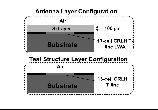
Based on the fabricated 13-cell CRLH T-line in Sec. 3.4.2, one 280-GHz LWA
is also implemented in the Global Foundry 65-nm C MOS process. P1 in Figure
3.10 is selected as the antenna input, and P2 is left open circuit. As shown
in Figure 8.4, a standard high-resistivity silicon layer (750 Ω · cm) with a
thickness o f 100 µm is placed on top of the antenna surface to enhanc e the
radiation efficiency.
8.4.1.2 2D Antenna Array Design
One sing le CRLH T- line (1 -D)-based LWA design in CMOS has limited gain
and radiation efficiency at THz. Meanwhile, a 1D leaky-wave structure pro-
duces a fan beam, narrow in the scan plane and fat in the transverse plane.
As for that, a 2D phased array by c ombining several 1D LWAs in an array
configuratio n naturally can lead to pencil beams and provide additional 2D
scanning capability, when using frequency scanning in the plane o f the LWA
structures and electronic scanning (typically used in conventional a rray phase
Antenna 203
Figure 8 .4: Stacking of high-resistivity Si layer on top of the LWA.
shifters) in the transverse plane as shown in Figure 8.5. The 2D array com-
poses of a shielded 1D 1 3-unit-cell CRLH T-line-based power divider feeding 4
identical 1D 13-unit-cell CRLH T-line-based LWAs. The CRLH T-line-based
power divider is identical to each of 4 CRLH T-line based LWAs in structure,
but radiation losses a re ignored due to a shielding layer on it. A THz signal
source drives the power divider from one terminal and the first four unit-cells
are used as matching networks to have maximized input power to multiple 1D
arrays.
8.4.1.3 EM Simulation
The proposed CRLH T-line-based LWA design is verified by EM simulation
in HFSS. As shown in Figure 8.6 , the maximum efficiency was 6.4% in 2 30 ∼
290 GHz, and it is enhanced to 40.5 ∼ 65.2% after stacking the dielectric layer
with high resistivity of Si. The maximum enhancement of 26 times is achieved.
After the enhanc ement of efficiency, the maximum antenna gain of 4.1 dBi is
achieved at 280GHz. As illustrated in the radiation pattern shown in Figure
8.7, a broadside radiation is observed at 280 GHz when β = 0. Note that the
zero phase propagation at 280 GHz also provides higher gain and efficiency
than the neg ative phase (β < 0 at 290 GHz) and positive phase (β > 0 at
250 GHz) propagation with tilted radiation direction. Note that the zero-β
frequency of 280GHz shown in Figure 8.7 is lower than the 303 GHz shown in
Figure 3.13. This is mainly because of the increase of equivalent p ermittivity
due to the stacking of a high- resistance silicon layer.

204 Design of CMOS Millimeter-Wave and Terahertz Integrated Circuits
2
3
4
plane steering
plane
steering
CRLH T-line as Leaky-Wave Antenna Array
CRLH T-line as Power divider
d y
Via bars(M1~LB) connected to ground
Y
X
X
Z
Y
Terminal
Terminal
Terminal
d x
Terminal
0
90
Phase
shifts for
/ 2
T-line
Power Divider
300GHz
Higher Gain
Terminal
300GHz
Source
Sheilded
Figure 8.5: Structure of CRLH T-line-based 2D phase-arrayed array
in THz.
Figure 8.6: Radiation efficiency enhancement by stacking a high-
resistivity Si layer.

Antenna 205
Figure 8.7: Gain radiation patterns for the proposed 1D LWA array
at three frequencies: f = 250 GHz (β < 0, backward radiation), f = 280
GHz (β = 0, broadside radiation), and f = 290 GHz (β > 0, forward
radiation).
5.1dBi
Figure 8.8: Gain radiation patterns for the proposed 2D LWA array
at three frequencies: f = 260 GHz, f = 280 GHz and f = 310 GHz.
Fig. 8.8 shows the EM simulation results of the 2D phase-arrayed LWA for
φ= 90
◦
plane. The proposed 2D array achieves a gain of 5.1 dBi at 280 GHz,
1 dB higher than 1D a rray to support longer transmission distance. Higher
gain improvement will be achieved if we can use a power divider with smaller
attenuation c onstant α. The proposed 2D array thereby can improve the gain
of antenna and also realize 2 dir ections for the frequency-dep endent beam
steering.

206 Design of CMOS Millimeter-Wave and Terahertz Integrated Circuits
Figure 8 .9: HFSS simul ation results o f proposed SIW antenna direc-
tivity at 270 GHz.
8.4.2 280-GHz SIW
8.4.2.1 Antenna Design
The proposed on-chip SIW antenna is designed in the 65nm CMOS proce ss
with 9 metal layers as shown in Figure 8.3. A composite dielectric material
with silicon dioxide (SiO
2
) and silicon nitride (Si
3
N
4
) is enclosed in the cuboid
cavity (410 µm × 410 µm × 9 µm) formed by the topmost aluminum layer
(AL), bottommost copper layer (M1) and metal walls constructed by metal
layers and via bars (M1-AL). The chip area required for SIW antenna is 0.17
mm
2
. Two 17-µm wide rectangular slots with different lengths (325 µm and
360 µm) are crossed at the center of the AL layer to create four resonance
modes with perpendicular polarization directions at 270 GHz. A rectangular
slot (120 µm × 30 µm) is cr eated at each corner to reduce the antenna size
at the desired operating frequency as dis cussed in Sec. 8.3. Different from the
SIW design in Printed Circuit Board (PCB), a uniform metallic plane is not
ava ilable in CMOS process ac cording to the metal density rules. As such, the
bottom side (M1) is implemented in mesh type with tiny squa re slots (3.5 ×
3.5 µm
2
) placed with 12-µm pitch. The antenna input is fed by a micro-strip
line with characteristic impedance of 40Ω, which is implemented by M8 and
M1 layers for signa l and ground, respectively.
..................Content has been hidden....................
You can't read the all page of ebook, please click here login for view all page.