

Introduction 9
dard CMOS technology is always considered as the most cost effective so lution
to combine all digital, analog and RF system designs. Moreover, CMOS-based
transmitter and receiver designs provide much higher flexibility in the power
amplification and frequency c ontrol. As such, the THz imaging can be di-
rectly performed in frequency domain with improved detection resolution and
efficiency. Therefore, it is of g reat interest to develop a CMOS-based THz
imaging system with high resolution, low cost and high p ortability.
1.3 CMOS THz Applications
1.3.1 THz CMOS Imaging
As shown in Figure 1.5, THz waves s uffer great loss when propagating inside
free space. As a result, the major challenges in the CMOS imaging system
design are to deal with the generation, transmission and detection of THz
signals. Take 300GHz signa l for example, assuming the power generated by
the signal source is -15 dBm and it suffers a free space path loss of about 80∼
90 dB for 1 meter distance, if the antennas on both transmitter and receiver
side can both provide 20dB gain, the se nsitivity of receiver must be better
than -85 dBm to detect the signal. Usually in a sta ndard CMOS process, the
transmitting power is limited by the maximum source drain voltage and the
current, the receiver sensitivity is limited by the noise figure and bandwidth
of receiver frontend, the gain and radiation efficiency of antennas are limited
Figure 1.5: Design challenges of THz imaging system to overcome the
huge path.
10 Design of CMOS Millimeter-Wave and Terahertz Integrated Circuits
by the loss of meta l and substrate and antenna size, respectively. In o rder to
overcome the above difficulties and des ign a high-performance THz imaging
system in CMOS process, the design of a high-Q passive structure is required
in every part of the ima ging system to replace the conversional tr ansmission
lines (T-line) or LC-tank resonators, which usually suffer fro m larg e size and
low quality facto r in THz and greatly limit the system pe rformance.
1.3.2 THz CMOS Communication
The ever-expanding data size in various applications and associated increasing
processing capability and memory size in mobile devices call fo r high-data -rate
communication systems which can handle multi-Gbps data rate with compac t
size and low p ower consumption at the order of hundreds of mW or less. For
example, the 5∼9GHz license-free band at 60 GHz is attractive to meet these
requirements.
For short distance communication with lower power consumption, nor-
mally line- of-sight set-up is used due to the high attenuation from passing
through (around 40∼5 0 dB) and reflection from (around 10∼20 dB) a wall.
As a result, the distance is normally targeted around ten meters or below to
cover the distance within a room.
Recently, there has been extens ive research on short distance THz com-
munication systems [36, 37, 38, 39, 40, 41, 42, 43, 44, 45]. The potential
applications are the wireless High Definition Media Interface (HDMI) where
you can have an uncompress ed high-definition movie transferred from laptop
and displayed on TV in real time; and Personal Area Network (PAN), wher e
a wire less link could be used to replace various cables used in home, and
connect all e lectronic devices together with high-data-rate router s to provide
smart house applications.
Compared with I II-V technologies, CMOS shows various advantages.
Firstly, a high integration c an be provided due to the lower power c onsump-
tion of digital signal processing in C MOS. A high integration also lowers cost
from multi-die package and improves performance with elimination of high-
frequency IOs. Secondly, a low cost can be obtained. In addition to the lower
fabrication cost compared with III-V technologies and lower package cost, the
testing cost c an also be lar gely reduced with built-in-self-test (BIST) inte-
grated on chip.
However, CMOS also brings various design challenges. For example, scaled
CMOS transistors with lower supply voltage in advanced technologies can
largely r educe size and dynamic power for digital processing. Unfortunately,
many Figure-of-Merits (FOMs) in the frontend such as output power, linear-
ity, and nois e all degrades along with reduced supply voltage. Furthermore,
large Process-Voltage-Temperature (PVT) variation tends to occur with ad-
vanced CMOS technologies, which makes RF design less accurate and poses
requirement on extra bandwidth to cover. These design challenges motivate
Introduction 11
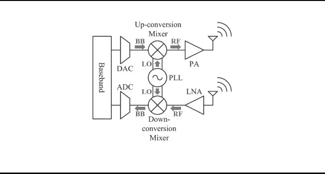
Figure 1.6: Simplified block diagram for a 60 GHz CMOS direct-
conversion transceiver front en d.
extensive researches on circuit and system innovations for 60GHz applications
in CMOS [36, 37, 38, 3 9, 40, 46, 47].
Direct conversion architecture has the a dvantage of energy efficiency and
was used for THz CMOS transceiver design in [48]. One simplified block dia-
gram is shown in Figur e 1.6 . On the transmitter side, baseband digital signal
is first converted to analog signal through a digital- to-analog convertor (DAC)
and then up-conve rted to RF signal by mixing with the carrier (LO) gener-
ated by PLL through a mix er. The resulted RF signal is then amplified by a
power amplifier (PA) and r adiated o ut through the antenna. On the receiver
side, the received RF signal from the antenna is first amplified by a low-noise
amplifier (LNA) and then down-converted to baseband signal by mixing the
corresponding LO generated by PLL through a mixer, which is further con-
verted to digital signal through an analog-to-digital convertor (ADC).
As THz waves suffer great path propagation in free space, the primary
challenge for THz communication system is to compensate the propagation
loss with consideration of multi-path effect of channel. Usually, one needs
to design a high-output power transmitter together with a high- sensitivity
receiver to compensate the path loss. The present THz wireless systems are
mainly single-input single-output (SISO) designs [49]. A wide-band and high-
gain hor n antenna is applied and is focused by aspherical Plano-convex lens to
compensate high path loss in point-to-point link. This approach is hard to be
integrated with the transceiver design. Recently, phase-arrayed multiple-input
multiple-output (MIMO) design [50] can be developed to overcome the hig h
path loss of the channel with a reaso nable budget in the THz band.
In the phase-array MIMO architecture, a beam is formed in a desired
direction by varying the relative delay in each element to compensate for
the difference in propagation delays for signals from different e lements. From
a THz wireless sy stem perspe ctive, both the EIPR (the effective isotropic

12 Design of CMOS Millimeter-Wave and Terahertz Integrated Circuits
Table 1.2: The Link Budget for THz Wireless Transmission System
at 0.3 THz
Norse floor (20 GHz bandwidth) -70.8 dBm
QPSK modulation (with 20G bps ) Eb/No=10dB @ B ER=10
−5
Tx
Unit transmitter output power -8 dBm
Effective antenna g ain 36 dBi
EIPR 28 dBm
Implementation loss 8 dB
Rx
Effective antenna g ain 36 dBi
Noise figure 10dB
Demo dulation los s 10 dB
Implementation loss 8 dB
Maximum allowed path loss 88.8 dB
Maximum available distance (for
amount link margin)
Around 5 m
radiated power) of the transmitter and s ensitivity of the r eceiver can be im-
proved in this MIMO architecture. For a n n-element massive array, the an-
tenna element is desig ne d with a gain of 5dBi at 280GHz (estimated from our
previous design [51]), the effective antenna gain is increased by 20 log
10
n. For
example, if output power of each transmitter of a 100-element array is -8dBm
for 280GHz mo dulated signal (estimated from our previous work [52]), the
maximum permitted EIRP of 28dBm can be achieved. For the receiver side,
the maximum antenna gain incense ment of 36dB (for n = 64) can be achieved;
this gain enhancement improves the signal strength (SNR) at the receiver side.
Exemplary link budget for 64-element phase-arrayed MIMO transmission link
at 30 0GHz can be seen in Table 1.2, which shows an enough link margin
for implementing a near-field (∼1m) THz wireless communication system by
massive THz MIMO architecture.
Note that phase-arrayed MIMO can be used in two different modes: spa-
tial diversity and spatial multiplexing. In spatial divers ity mode, the same
information is encoded into all transmit streams in such a way as to improve
range of coverage. For low-frequency cellular network, divers ity is often a p-
plied at receiving side of base station, because it is up-link limited in that
scenario. An example of receiver spatial diversity is Maximal Ratio Combin-
ing (MRC); the signals from all receiver antennas are combined after first
re-aligning their phases [53]. In spatial multiplexing mode, on the other hand,
the transmission antennas simultaneously tra nsmit independent signals over
the same frequency channel, resulting in an increase d spectral efficiency. In
low-frequency applications, such as WLAN and cellular network, spatial mul-
tiplexing is widely applied in line-of-sight environment to support higher data
rate with improved system capacity. For short-range THz high-speed wireless
communication, phase-arrayed MIMO technique is more attractive. However,

Introduction 13
Tx
Tx
Tx
. . .
MIMO
Beamfor
ming
control
&
Mode
control
Tx
Tx
Tx
. . .
MIMO
Beamfor
ming
control
&
Mode
control
BB_1
BB_2
BB_n
LOS Channel
(Channel Matrix H)
Spatial multiplexing for
capacity enhancement
(a)
Tx
Tx
Tx
. . .
MIMO
Beamforming
control
&
Mode control
Tx
Tx
Tx
. . .
MIMO
Beamformi ng
control
&
Mode control
NLOS Channel
(with obstacle)
Spatial diversity for
quality enhancement
(b)
Figure 1.7: Two massive MIMO modes proposed for THz wireless
link. (a) Spatial multiplexing mode in LOS scenario; (b) Spatial di-
versity mode in NLOS scenario.
different transmission scenarios are faced and have shown different character-
istics compared to tha t in the low-frequency band. These differences inspire
novel massive MIMO mechanism for THz wireless link. Fo r different transmis-
sion scenarios, the following can be applied for performance e nhancement.
For LOS (Line-of-Sight) transmission, spatial multiplexing mode
MIMO is applied as shown in Fig 1.7(a). Data of multiple users are
transmitted simultaneously by each transmitter; and each rece iver re-
ceives all transmitted data and separates (decode) them correctly for
..................Content has been hidden....................
You can't read the all page of ebook, please click here login for view all page.