

Power Combiner 173
(a) (b)
Figure 7.21: Comparator topologies for ADC design: (a) n-type; (b)
p-type.
Q0 =
D6 ·
D4 ·
D2 · D1 + D3
+ D5
+ D7
Q1 =
D5 · D4 · (D2 + D3) + D6 + D7
Q2 = D4 + D5 + D6 + D7.
(7.10)
Note the digital inputs and their inverts
DX are passed to the encoder
through transmiss ion gates and inverto rs to ensure a similar time delay.
3-Bit DAC
The DAC is used to c ontrol the PA’s biasing current based on input digital
signals. A simple comparator is designed to switch different biasing currents.
As shown in Figure 7.23, by using 3 comparators, the obtained biasing current
I
b
can be controlled by the DAC inputs:
I
b
= I
ref
× (4 · DAC3 + 2 · DAC2 + 1 · DAC1) , (7.11)
where DAC3, DAC2, and DAC1 are the 3-bit digital input, with which the
biasing current can be varie d from I
ref
to 7I
ref
.
7.4 Circuit Prototyping and Measurement
7.4.1 60 GHz PA Design with Single-Ended 2×2
Power Combining
One 60GHz Pt prototype with proposed 2D distributed power combining is
implemented in UMC 65nm logic and mixed-mode low leakage low-K CMOS

174 Design of CMOS Millimeter-Wave and Terahertz Integrated Circuits
(a)
(b)
(c)
Figure 7 .22: 8-to-3 encoder for ADC design: (a) Q0, (b) Q1, (c) Q2.
technology with 6-metal layers (1 thick metal layer). The circuit is des igned
and verified by EM simulation (ADS-Momentum) before fabrication.
7.4.1.1 60GHz PA Design
With ZP S des igned and characterized, the pro posed 2D distributed power
combining network is implemented in a PA for demonstration [224]. As shown
in Figure 7.24, a 2-sta ge PA is designe d with a single transistor in the 1st

Power Combiner 175
Figure 7 .23: DAC topology.
Figure 7.24: Schematic of 2-stage PA with a 2×2 distributed power
combining network.
stage a s a driver; and a 2×2 distributed power combining a rray in the 2nd
stage, which has 2 power-combining branches and each branch has a 2-stage
SEDFDA. All transistors are in single-ended common-source top ology w ith
transistor s ize of 64×1µm/60nm. With a biasing current of 22mA, the simu-
lated f
t
is 172 GHz. The parasitic capacitances from transistor gate and drain
are absorb ed during the ZPS design to realize the distributed amplification.
As a result, the shunt inductor (L
p
) in Figure 2.5(b) is resized to a single loop.
176 Design of CMOS Millimeter-Wave and Terahertz Integrated Circuits
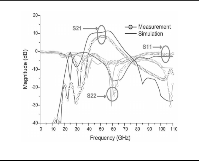
Figure 7.25: Simulated and measured S parameters o f PA under 1.2
V supply.
Notice the size of L
s
in the gate line is smaller than in the drain line due to
a larger parasitic capacitance at transistor gate.
The power combiner implemented in the 2
nd
stage only has 2 branches,
mainly due to limitation of the tape-out area. More branches can be used to
enhance the p ower performance. Moreover, CPW transmiss ion lines are used
as parallel inductors for matching and DC biasing at the same time, therefore
no additional biasing circuit is required.
7.4.1.2 Simulation and Measurement Results
Circuit simulation is done in both Cadence and ADS. The chip is meas ured on
a CASCADE Microtech Elite-300 probe station and Agilent PNA-X (N5247A)
with frequency-sweep up to 11 0GHz. Me asurement for PA power performance
is done a t the center frequency (52GHz) with pads de-embedded.
Figure 7.25 shows the simulated and measured S parameters. An open-
short de -embedding was performed to obtain the results. From simulation,
the maximum gain is at 56.3 GHz with 11.3 dB. A 3-dB bandwidth of 2 1GHz
is achieved (40.3GHz ∼ 61.7GHz). At 60GHz, a 9.8- dB ga in is obtained. The
measured gain, on the other hand, has a peak value of 8.3 dB at 52 GHz. The
3-dB BW is 16GHz (44 to 60GHz). Compared with simulation, the center fre-

Power Combiner 177
Figure 7.26: Reverse isolation and stability of PA under 1.2 V supply.
quency is not s hifted much, but power gain drops 3dB and bandwidth shrinks
5 GHz. Output matching co nfirms with the simulation while degradation oc-
curs at the input matching. This input misma tch may be due to lack of device
modeling, a nd can be used to justify the reduction o f power gain.
The measured reverse isolation and stability for PA are shown in Fig ure
7.26. The circuit is unconditionally stable from DC to 110GHz, with reverse
isolation better than -25 dB over the entire range.
In addition, Figure 7.27 s hows the measure d power p erformance at center
frequency (52GHz). With 1.2-V supply, OP
1dB
of 9.7 dBm and t
sat
of 11 dBm
are achieved. PAE dro ps to 7.1%. Note that both PAE and output power are
limited by the number of power combining branches and dis tributed stages,
and can be further improved when a larger 2D power combining network is
employed, as will be demonstrated in the following sections.
Furthermore, Table 7.1 summarizes the presented work with comparison
to the state-of-the-art 2-stage CMOS PAs at 60 GHz. Comparison shows that
the proposed PA c an achieve the state-of-the-art performance for all FOMs.
Lastly, Figure 7.2 8 shows the chip microgr aph. Including pads, the PA
occupies an area of 0.39 mm
2
, which is quite compact when compared to the
traditional design with the use of T-line. Note that the upper part of the
photo is the 60GHz PA w ith 2×2 power combining network. The lower pa rt
of the photo is the de-embedding structures used to characterize the CRLH
T-line-based zero- phase-shifter.
..................Content has been hidden....................
You can't read the all page of ebook, please click here login for view all page.