
Oscillator 99
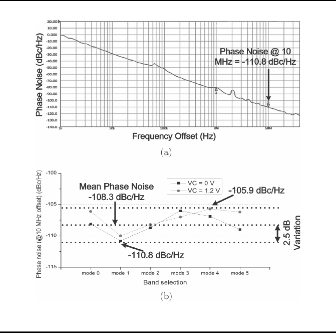
Figure 4.28: Measured phase noise performance for the 60-GHz s ym-
metric VCO. (a) Phase noise at 60.8 GHz. (b) Phase no ise variation
for all selection modes.
[63]. Note a higher fr equency is adopted to further demonstrate the advantages
of CRLH T-line at higher frequencie s.
4.4.3.1 90GHz VCO Design
The proposed tunable CRLH T-line-based Mobius-ring RTW-VCO shown in
Figure 4.13(a) is fabricated in 6 5-nm CMOS Global Foundries 1P8M RF
CMOS technology as shown in Figure 4.30(a). To push the cut-off frequen-
cies away from operation frequency region, each stage is implemented with
2 distributed CRLH T-lone unit-c ells. As a result, 180-degree phase shift is
required due to the Mobius-ring connection, which leads to a 90-degree phas e
shift in each unit-cell. The EM simulation results for the designed unit-cell are
shown in Figure 4.30(b). At the frequenc y of interest 100 GHz, one unit-cell
can provide 90-degree phase-shift with loss at -1.86 dB, which is compensated
by the negative resistors realized by a cros s-coupled pair. Note the unit-cell

100 Design of CMOS Millimeter-Wave and Terahertz Integrated Circuits
Figure 4.29: Measured output spe ctrum of equally spaced starting
frequencies under 6 different modes for the 60-GHz symmetric VCO.
Table 4.10: Performance Summary and Comparison of Wide-Tuning
60-GHz VCOs
[135] [134] [136] Asym.
VCO
Prototype
Sym.
VCO
Prototype
Technology (CMOS) 90 nm 65nm 65 nm 65 nm 65 nm
Freq. (GHz) f
OSC
76.5 70.2 77 59.6 61
Freq. Tuning Range
(%)
FTR 7.0 9.6 14.5 25.8 14.2
Phase Noise
(dBc/Hz)
PN -110.6 -106.0 -112 -106.7 -110.8
Phase Noise Mean
(dBc/Hz)
P N -107.1 -99.5 -108.5 -98.5 -108.3
Phase Noise
Variation (dB)
σ
P N
3.5 6.5 3.5 8.2 2.5
Power (mW) P
DC
19.4 5.4 190 5.4 6.0
Area (mm
2
) A 0.01 0.003 0.15 0.031 0. 031
Figure of Me r it
(dBc/Hz)
FOM
(1)
-171.9 -169.1 -163.4 -166.7 -176.2
Figure of Me r it
(dBc/Hz)
FOM
t
(2)
-168.8 -168.8 -166.7 -174.9 -179.3
(1)
F OM = P N − 20 log
f
OSC
∆f
+ 10log(P
DC
/1mW )
(2)
F OM
t
= P N − 20 log
f
OSC
∆f
×
F T R
10
+ 10log(P
DC
/1mW )

Oscillator 101
(a)
(b)
Figure 4.30: (a) Die micrograph of the proposed VCO. (b) The EM
simulation for one CRLH T-line unit-cell. Note that Lp is shared by
two unit-cells and its value is purposely designed doubl ed.
is biased to opera ting in the LH re gion, with the resonant mode in the RH
region (-90-degree phase shift) highly suppre ssed.
4.4.3.2 Simulation and Measurement Results
The proposed VCO is fabricated 65 -nm CMO S Global Foundries 1P8M RF
CMOS technology. The VCO core area is about 0.0812mm
2
. The output spec-
trum is measured by E4408B spectrum analyzer through one 11970W har-
monic mixer. The supply voltage for buffer is 1.2 V and for VCO is 1 V. The
measured current for the core VCO is 14 mA.
Figure 4 .31: Measured frequency tuning range by 4 sub-b ands.

102 Design of CMOS Millimeter-Wave and Terahertz Integrated Circuits
Figure 4.32: Measured phase noise at 82.22 GHz with 10 MHz offset
frequency.
As shown in Figure 4.31, by using the proposed tuna ble CRLH T-line, a
wide FTR of 29.6% is achieved from 76.59GHz to 102.01GHz, with a center
frequency at 89.33 GHz. The full FTR is formed from the four sub-bands
controlled by two switches: (75.67–83.11GHz), (7 9.65–87.78GHz), (86.18–94
GHz) and (93.89–102.01 GHz). With a tuning voltage for varactor from 0 V
to 1.2 V, each sub-band is fully covered. The measured phase noise varies
from −100.1 dBc/Hz to −98.7 dBc/Hz with a sample plot shown in Figure
4.32, where 6–9 dB deviation is observed compared with simulation, which
may be due to inaccurate device and noise models at such high frequency and
imperfect ground provided during measurement. T he measur ed output power
is from -23 dBm to -15 dBm as shown in Figure 4.33. The output power
variation is about 8 dBm.
As summariz ed in Table 4.11, the performance of the proposed VCO is
further compared with other published millimeter-wave VCOs in 65nm CMOS
technology. According to the Table 4.11, the phase noise is comparable with
others, and the wide st FTR and the best FOM
T
are achieved by the proposed
VCO.
F OM = P N − 20 log
f
OSC
∆f
+ 10log(P
DC
/1mW )
F OM
T
= P N − 20 log
f
OSC
∆f
×
F T R
10
+ 10log(P
DC
/1mW ).
..................Content has been hidden....................
You can't read the all page of ebook, please click here login for view all page.