

304 Design of CMOS Millimeter-Wave and Terahertz Integrated Circuits
6
-45
-40
-35
-30
-25
-20
-15
-10
-5
0
S21 (dB)
Frequency (THz)
h=4um
h=7um
h=10um
h=13um
(a) (b)
1 2 3 4 5
100 200 300 400 500 600 700 800
-10
-9
-8
-7
-6
-5
-4
-3
-2
-1
insertion loss (dB)
Frequency (GHz)
1mm SPP T-line
1mm Conventional T-line
3mm SPP T-line
3mm Conventional T-line
Figure 14.5: (a) Simulated transmission coefficient of the SPP guided
wave as a fun ction of the groove depth h with a = 2.4 µm, w = 5 µm,
d = 15 µm, (b) comparison of simulated insertion loss for both SPP
T-line and conventional T-line with different length.
effect on the shielding of E-field from T-line to the substrate, it inherently in-
troduces significant crosstalk into the near by conductors through the current
flowing onto the ground surface, which will be even worse as frequency rises.
All these feature s manifest the T-line as an unsuitable ca ndidate for on-chip
interconnects in a high-speed wireline system.
To obtain low reflection, a bending copla nar waveguide (CPW) converter
using the gradient co rrugation grooves and flaring g round [294] is employed
to realize momentum matching between SPP interconnect and other devices,
such as a transformer or modulator , as illustrated in Figures 14.4(a) and (b).
Note that in the plasmonic waveguide only SPP modes are supported with E
z
component remaining strong along the x directio n, leading to a momentum
mismatch (k
x
6=k
0
) at the interface. As a result, a gradient CP W, w hich guides
and confines the quasi-TEM wave along the y direction betwee n signal trace
and ground, gradually transforms the guided wave to SP P mode, or vice versa.
The E-fie ld distribution of such conve rsion is conceptually illustrated in Figure
14.4(b). Due to limitation of the CMOS process, a linearly gradient model is
used. Figure 14.4 (c) shows the input reflection coefficient (S
11
) of the SPP
T-line with converter loaded by 50 Ω resistance at both sides, which indicates
wide-band impedance matching for different lengths of wire. The gap of CPW
and the gra die nt factor are both optimized during the design phase of the I/O
transceiver for maximum matching efficiency between functional blocks.
Next, we examine the transmiss ion property of on-chip SPP T-line with
compariso n to that of conventional T-line s tructure. While the bandwidth of
conventional T-line is largely affected by the highly conductive substrate at
THz, the asymptotic frequency of surface plasma is mainly determined by the
metal structure. To verify this, we begin by examining the spectral transmis-
CMOS THz Wireline Communication 305
sion properties of designed SPP T-line up to several T Hz. In Figure 14.5(a),
we show the simulated wide-band transmission spectra with h = 4, 7, 10 and
13 µm. There are a few of notable characteristics in these spectr a. As observed,
when the grooves are very shallow (i.e., 7µm deep or les s), despite an obvious
high-frequency cuto ff, the SPP T-line transmission spectra appear to be rela-
tively broa dband. As the groove de pth begins to increa se, both the line width
and cut-off frequency of this resonanc e decrease. As the groove depth further
increases, the single wide-band transmission resonance is replaced by multiple
narrowband transmission resonances. In the theoretica l limit of transmission
by guided SPPs, there are no modes appearing at frequencies above the Bragg
frequency f
B
= c/2d, where c is the speed of light. Here, the anti-resonance
(AR) frequenc y, which is used to characteriz e the frequency corresponding to
the signal being sharply attenuated, can be applied to e xplain the transmis-
sion properties of the periodica l curvature structures due to Fano -interference
phenomenon [3 03]. Even so, the transmission maintains low loss and wide
band at the frequency far below the AR frequency. We then compare the
transmission for both T-line str uc tures at frequencies less than 1 THz, where
the advanced integrated circuits normally opera te. With low return loss, the
loss of the SPP T-line is mainly contributed by the metal resistive loss. Figure
14.5 (b) shows the comparison results. Clearly, the transmission of SPP T-line
has very wide bandwidth with low loss, whereas the conventional T-line suffers
from strong attenuation in THz. This observation confirms the insensitivity of
guided wave to the low-resistive substrate profile. Specifically, the 3-mm long
SPP T-line is almost 3 times that of its 1 mm counterpart across a very wide
band, similar to cascading of thr ee 1-mm unit-cells. However, the 3-mm-long
traditional T-line has much larger attenuation than the loss added by three
1-mm unit-cells, illustrating its vulnerability to lossy substrate. As a result, by
properly structuring the top metal, the loss of SPP T-line can be minimized
across the wide ba nd, which cannot be achieved by a ba re T-line in CMOS
at THz. We then estimate how long the on-chip SPP T -line can support the
THz signal by transforming the S parameter s to the attenuation c onstant.
The resulting propagation length of the lowest-order mode can be readily ob-
tained. It shows that the attenuation constant along the pointing vector is
around 1 cm
−1
, leading to about 1 ∼ 2 cm e
−1
-decay length for propagation,
which satisfies most on-chip wireline communication. Simulations further re-
veal that an increas e of groove depth brings about long er pr opagation length,
in consistent with the observation that the propagating modes are now more
restricted to propagating only along the corrugated surface of interconnect.
In other words, more energy is conserved by reinforcing the confinement of
the guided mode. Note that this experiment has not incorp orated the plane
wave-to-surface wave converter design, which is bulky and hence not suitable
for on-chip realiz ation. In the design without a converter, the resulting trans-
mission bandwidth will be reduced, as stated befo re. Fortunately, the advance
mm-wave circuitries operate at frequencies far away from the asymptotic fre-
quency, which provides great margin to consider only the low frequency r egion.

306 Design of CMOS Millimeter-Wave and Terahertz Integrated Circuits
(a)
(b)
(c)
Agilent PNA-X
VDI
(220GHz-325GHz)
Powe
Supply
VDI
(220GHz-325GHz)
Powe
Supply
S Parameters
Golden
Waveguide
Golden
Waveguide
DUT
400µm
400µm
225µm
(d)
Figure 14.6: (a and b) The simulated electrical field distribution on
the cross-section for both SPP and T-line coupl er in 65 nm CMOS
technology, the parameters configuration is the same as in Fi gure
14.2. The left-handed side T -l ine is the aggressor with EM filed e xci-
tation at one terminal with the other termination loaded with 50 Ω
impedances, and the right h and side T-line is the victim trace with
both ends terminated by 50 Ω impedances, (c) measu rement setup for
the THz SPP coupler, (d) die micrograph o f the SPP-based coupler
in 65 nm CMOS for Terahertzes applications.
For this reason, the converter is not necessary, and the design of on-chip SPP
interconnections becomes much more re laxed.
Crosstalk arises from the interaction of E M fields generated by adjacent
data signals when they propagate through T-lines and connectors. For exam-
ple, wiring c apacitances of o n-chip interconnect tend to dominate c rosstalk a nd
backplane connectors induce multi-pin crosstalk. Recent work has addressed
crosstalk equaliza tion issues between neighboring serial links by an effo rt of
crosstalk neutr alization techniques [304]. Crosstalk c onsiderations also affect
CMOS THz Wireline Communication 307
the performanc e of integrated digital circuits, which can be partially alleviated
by equa lizing the crosstalk-induced timing jitter. However, all these methods
consume considerable power with the data rate only limited to multi-gigabit
per second. Owing to the advantage to control the propag ation property of
EM energy, we expect that interconnects realized by SPP T-line present less
crosstalk . Recall that for a guided wave structure, the energy associated with
the guide mode was highly confined near the surface, with the field decaying
evanesc ently within the apertures. While the guided mo de is excited along
the metal surfa ce, e lectromagnetic couplings to both substrate and adjacent
conductors are strongly attenuated. As such, the complexity of circuit imple-
mentations can be relaxed. To verify this, two SPP T-lines are pla ced clos ely
back-to-back to form an on-chip SPP-based coupler. All physical dimensions
are the same as before with spacing as 2.4 µm. Figure 14.6(a) shows the E-
field distribution and the conventional coupler realiz ed by T-line with 2.4µm
spacing is shown in Figure 14.6(b) for compariso n. In this experiment, the
left-hand side T-line is the a ggressor with 300 GHz TEM wave excitation at
one terminal, and the right-hand side T-line is the victim. The other three
ports are terminated by 50 Ω impedances. As predicted, the local E-field in-
tensity |E
tntal
| is locally confined by the corrugation structur e with only small
portion of ener gy to spread out, while it strongly radiates out in the case of
the traditional T-line coupler. As a result, the SPP coupler confines more en-
ergy and has less coupling to the victim trace, leading to significant crossta lk
reduction. The mea surement results with respect to the cros stalk reduction
will be given in the next section.
To demonstrate the superior performance in crosstalk reduction by the
SPP-based coupler, the measured S-parameters are shown in Figure 14.6.
First of all, to have a fair comparison with the direc tional c oupler realized
by conventional T-line, the simulation results of the SPP coupler are fit to
the measurement ones (S
11
and S
41
). After the parameter fitting is done,
the conventional T-line coupler is simulated using the same substrate profile.
The T-line co upler also has a meandering shape that resembles the structure
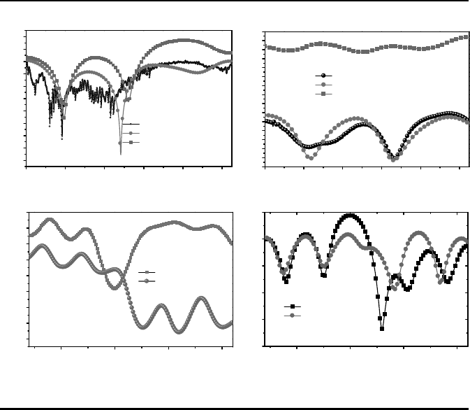
shown in Figure 14.6(d). The measured and simulated reflection coefficient
(S
11
) is shown in Figure 14.7(a) with comparison to the T-line coupler. The
measured S
11
is below -14 dB over 220–325 GHz, showing wide-band reflec-
tion coefficient. The fitting of S
11
is below -14 dB over 220–325 GHz, showing
wide-band reflection coefficient. The fitting of S
11
is also presented, which
has only a small deviation from the measurement result. As a comparison,
the S
11
of the traditional T-line coupler becomes poor in the vicinity of 300
GHz which is almost -5 dB, re sulting in the refle ction of over 30% of the
electromagne tic waves. Considering that the T-line is natur ally wide-band,
the reason for impedance mismatches is due to the strong coupling, which is
further verified by Figure 14.7(b). As shown, the measured crosstalk (S
41
) of
the proposed structure is lower than -24 dB which is o n avera ge 19 dB better
than that of the traditional T-line coupler across 220–325 GHz, illustrating
great improvement in crosstalk reduction. In addition, the crosstalk is no t
308 Design of CMOS Millimeter-Wave and Terahertz Integrated Circuits
(a)
(c)
(b)
(d)
220 240 260 280 300 320
-36
-34
-32
-30
-28
-26
-24
-22
-20
-18
-16
-14
-12
-10
-8
-6
Crosstalk (dB)
Frequency (GHz)
Measured SPP Coupler
Simulated SPP Coupler
Simulation T-Line Coupler
250 300 350 400
-6.5
-6.0
-5.5
-5.0
-4.5
-4.0
-3.5
-3.0
-2.5
Insertion Loss (dB)
Frequency (GHz)
SPP Coupler
TLine Coupler
220 240 260 280 300 320
-55
-50
-45
-40
-35
-30
-25
-20
-15
-10
-5
S11 (dB)
Frequency (GHz)
Measured SPP Coupler
Simulated SPP Coupler
Simulation T-Line Coupler
250 300 350 400
-30
-25
-20
-15
-10
-5
S31 (dB)
Frequency (GHz)
SPP Coupler
TLine Coupler
Figure 14.7: (a) Th e measured and simu lated results of the input re-
flection coefficient (S
11
) for the SPP coupler, and the simulated S
11
of
the T-line coupler. The S p arameter extraction for the T-line coupler
is performed after the parameter fitting is done, (b) the measured
and simulated result of the crosstalk (S
41
) for the SPP coupler, and
the simulation result for the conventional T-line coupler as a com-
parison, (c) the simulated insertion loss (S
21
) for both SPP/T-line
couplers, and (d) the simulated near-ended coupling (S
31
) for both
SPP/T-line coupler.
obviously degraded as the frequency goes up while it beco mes significantly
worse for the traditional T-line coupler, implying wider bandwidth achieved
by the SPP-based coupler. For example, the crosstalk is only -25 dB obtaine d
by the SPP-based coupler at 325 GHz but it rises to -7 dB by the T-line coun-
terpart. That is to say, about 20% of the EM energy is coupled to the victim
in the traditio nal T-line coupler but only 0.3% energy leaks to the victim in
the SPP-based coupler. The simulated crosstalk of the SPP-based coupler is
given in the same figure as well which shows good agreement with the mea-
surement result. The small discrepancy may be due to the 10% dummy fill
or process varia tion that have not been taken into account during the simu-
lation setup. Combined with Figure 14.7(a), we can observe that the surface
..................Content has been hidden....................
You can't read the all page of ebook, please click here login for view all page.