

72 Design of CMOS Millimeter-Wave and Terahertz Integrated Circuits
Figure 4.5: Proposed new inductor-loaded transformer by switching
current return-paths with only one transformer.
However, the large layout size of the loop inductor and str ong ma gnetic cou-
pling with adjacent devices limit the numb er of tra nsformers. Moreover, as
more transformers are used, magnetic coupling fro m different transformers
tend to cancel each other, and hence make the tuning less effective. As a re-
sult, the number of sub- bands achieved by the conventional inductor-loaded
transformer topology often limits to 4 (with 2 transformers used) and below.
In this section, a new inductor-loaded transformer topology is propos ed,
which breaks throug h the limit of the conventional inductive tuning. The
concept of the proposed topology can be explained in Figure 4.5. Only one
transformer is used for the new inductor-loaded transformer, with switches
placed at various locations of the secondary co il. When some combination of
switches are turned on such that a closed-loop is constructed in the secondary
coil, a current retur n-path fo rms. Different-sized current retur n-paths generate
different magnetic fluxes, which are fed back to the primary coil and hence
result in multiple sub-bands.
4.2.2.1 Comparison with Traditional Loaded Transformers
Since the proposed topology can increase the numbe r of sub- bands by simply
adding more switches, the sub-band number can be easily designed to be
larger than 4 with compact layout area when compared to the c onventional
inductor-loaded transformer.
Moreover, different from the r esistor-loaded transformer tha t has a highly
nonlinear tuning-curve and large K
V CO
, the new inductor-loaded transfor mer
achieves a much smaller K
V CO
through multi-sub-band operation within lin-
ear tuning-curve. As a result, the phase nois e performance can be improved
with no PLL locking difficulty. The small K
V CO
may also be used to trade
for a wider tuning range, w hich can be easily realized by implementing with
a large coupling fac tor k, as explained in (4.7).
In addition, as mentioned in Section 4.2.2, frequency-tuning for capacitor-
loaded transformer is realized by varying the value of C and thus ω
2
. However,

Oscillator 73
Table 4.2: Trade-Offs b etween Different Loaded Transformer Topolo-
gies
Topology Benefits Limitations
R-loaded transformer • wide tuning range large
sub-band number
large effective K
V CO
• large sub-band number
C-loaded transformer • large sub-bend number limited tuning range
Traditional L-loader
transformer
• wide tu ning range limited su b-band
number
Proposed L-loaded
transformer
• wide tu ning range asymmetric current
return path
according to (4.6), as C increases or ω
2
drops, Q
eq
is severely degraded. As
a result, the FTR that can b e achieved is limited. Furthermore, the FTR for
the varactor or capacitor-bank is further limited by parasitic capacitance from
switches and transfo rmers.
Trade-offs between different loaded-transformer topologies are summarized
in Table 4.2. However, one des ign challenge is how to deal with asymmetric
current retur n-paths in certain sub-bands, which will be discussed in detail in
Section 4.4.3.
4.2.2.2 Model of Proposed New I nductor-Loaded Transformer with
Switches
Similar to the modeling or conventional inductor-loaded transformer, a more
comprehensive circuit model is develop ed in Figure 4.6 for the proposed new
inductor-loaded transformer which can take the parasitic effects from the off
part of the secondary coil into consideration.
Figure 4.6 shows the circuit models for the proposed inductor-loaded trans-
former. Its se condary coil is split into two portions: L
2
and L
3
. The L
3
portion
is switched on to form a current return-path to generate feedback to L
1
, while
the remaining portion of the secondary coil (L
2
) is left floating by keeping the
switch terminating L
2
off. The change of loaded inductance is then e mulated
by varying the ratio between L
2
and L
3
. The r esulted L
eq
and R
eq
can then
be calculated by solving the following equations:
I
1
= V
1
×
1
R
eq
+
1
sL
eq
+
i
neq
V
1
= sL
1
I
1
+ sM
12
I
2
+ sM
13
I
3
V
2
= sM
12
I
1
+ sL
2
I
2
+ sM
23
I
3
V
3
= sM
13
I
1
+ sM
23
I
2
+ sL
3
I
3
V
2
+ V
3
+
R
2
I
2
1+sR
2
C
2
=
R
2
i
n2
1+sR
2
C
2
V
3
+
R
3
(I
3
−I
2
)
1+sR
3
C
3
=
R
3
i
n3
1+sR
3
C
3
.
(4.9)

74 Design of CMOS Millimeter-Wave and Terahertz Integrated Circuits
Figure 4.6: Equivalent circuit model for the proposed loaded trans-
former.
4.2.2.3 Performance Study
Based on the previously developed switch a nd transformer models, perfor-
mance for the proposed inductor-loaded transformer topology can be further
analyzed to o btain the optimized design with respect to switch sizing W
s
.
With extracted switch parameters such as in Table 4.1, switch pe rformance
under various sizes W
s
can be studied. Based on the design pa rameters sum-
marized in Table 4.3, we have the following detailed performance study.
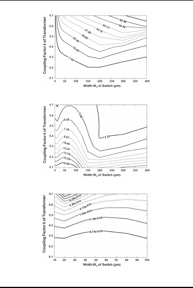
Firstly, the impact of switches on the FTR performance is studied in Figure
4.7(a). Confirmed with our conclusion in (4.7), a larger coupling factor k leads
to a wider FTR. When s w itch size is small, the FTR is also observed to increa se
with switch size. This can be ex plained by the analysis in Section 4.2.2, where
a larger C
on
would raise the FTR when R
off
is sufficiently large. However, as
switch size further increases, R
off
becomes too small to fully switch o ff the
current return path, and FTR sta rts to decrease.
Secondly, the impact of switches to phase noise performance can be also
analyzed. Switches on a loaded transformer degrade the phase noise perfor-
mance from two aspects. It can decrease output signal power by reducing the
effective Q factor in LC-tank; and also increase phase noise by transferring
noise power to output node s. These two aspects are analyzed in Figure 4.7(b)
Table 4.3: Parameters for 60-GHz VCO Desig n Based on Proposed
Loaded Transformer Topology
Switch Transformer Other
W
s
(µm) L
prim
(pH) L
sec
(pH) k C
t
(fF)
10˜400 80 80 0.1˜0.7 100
Oscillator 75
(a)
(b)
(c)
Figure 4.7: Design optimization for (a) frequency tuning range (%),
(b) the minimum quality factor in the tuning range, and (c) the max-
imum output noise spectral d ensity at 10 MHz offset in tuning range.

76 Design of CMOS Millimeter-Wave and Terahertz Integrated Circuits
and (c), by examining the minimum Q factor of the LC- tank and the maxi-
mum output noise spectral density at the offset frequency. One can obser ve
that there is an optimal switch size for the minimum phase noise degradation.
4.2.2.4 Design Optimization Flow
As such, we present a design flow in Figure 4.8 to optimize the specific perfor-
mances of the proposed inductor-loaded transformer topo logy. The targeted
frequency (freq.) and tuning range (FTR) define the minimum frequency
(f
min
) and ma ximum frequency (f
max
) to be desig ne d. With the proposed
tuning topology, f
min
is mainly determined by the inductance of the pr imary
coil (L
prim
) and the total capacitance in LC-tank (C
t
). Due to the single-
loop topology adopted for the proposed transformer, the inductance on its
secondary coil (L
sec
) can be acco rdingly determined.
Firstly, with the given FTR and targeted K
V CO
, we can calculate the
number of sub-bands (N
band
) needed, thus determining how many switches
are required as well as their locations on the secondary coil. Each sub-band
is then to be fully covered by a varactor pair as fine tuning. The refore the
tuning capacitance (C
tune
) is determined for vara ctor design. Besides C
tune
,
the rest part of C
t
is mainly contributed from the parasitic capacita nc e in the
cross-c oupled transistors, which can help determine the transisto r sizes.
Next, given L
prim
, L
sec
, and C
t
, f
max
is mainly de termined by the coupling
factor k of the transfor mer. For a sp ecific k value, an optimized switch size
can be found to minimize the phase noise (PN ) as Figure 4.7 (b) and (c)
shows. Note that since both phase noise and power consumption are related
Figure 4.8: Design optimization flow for wide-tuning VCO based on
the propos ed inductor-loaded transformer, where perfo rmance met-
rics are frequency, FTR, K
V CO
, power, and phase noise.
..................Content has been hidden....................
You can't read the all page of ebook, please click here login for view all page.