
178 Design of CMOS Millimeter-Wave and Terahertz Integrated Circuits
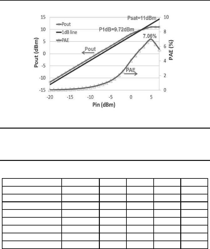
Figure 7.27: Measured power and PAE of PA at 52 GHz under 1. 2 V
supply.
Table 7.1: Comparison of State-of-the-Art Two-Stage 60 GHz CMOS
PAs
This Work
[192] [212] [193] [211]
Tech. (CMOS)
65nm 65nm 45nm 90nm 90nm
Supply (V)
1.2 1.2 1.1 1 1
Gain (dB)
8.3 14.3 6 8.2 5.6
OP
1dB
(dBm)
9.7 11 11 10.1 9
P
sat
(dBm)
11 16.6 13.8 11.6 12.3
PAE (%)
7.1 4.6 7 11.5 8.8
BW
−3dB
(GHz)
16 15 19 13 22
Area (mm
2
)
0.39
0.46* 0.06*
1.03 0.25
*Excluding pads
In summary, the presented simulation and measurement results have
demonstrated the feasibility of the proposed 2D distributed power combin-
ing as well as the implementation of metamaterial in the mm-wave region by
65nm CMOS technology.
7.4.2 60 GHw PA Design with Differential 2×4
Power Combining
The proposed 2D power combining network with the use of CRLH T-line-based
ZPS is demonstrated in the above section, proving its feasibility for 60GHz

Power Combiner 179
Figure 7 .28: Die micrograph with block illustrations.
CMOS PA design. However, due to the single-ended topology with a large
matching network deployed, the benefit to achieve wide-band and high output
power density is still not fully demonstrated. In this prototype, a differential
power combining network is implemented in 65nm CMOS technology with
improved performances in both power density and bandwidth [225].
7.4.2.1 60GHz PA Design
Differential CRLH T-lines presented in Section 3.2.3 are first designed and im-
plemented in both gate a nd drain lines in the 2D active CRLH T-line network
to obtain zero-phase-shift with circuit and layout diagrams shown in Figure
7.29. The parasitic capacitances from transistor gate and drain are absor bed
in ZPS design. The designed CRLH T-lines can realize zero-phase shift at
60GHz with compact s ize of 61µm×81µm and 76µm×81µm in gate and drain
lines, re spectively. Note a smaller L
p
is implemented in ra te line compared to
drain line due to lar ger parasitic capacitance on transistor gate compared to
transistor drain.
With the designed differential Z PS, one 3-s tage PA is implemented with
the central frequency at 63GHz in 65nm CMOS from Global Foundries 1P8M
RF CMOS technology, as shown in Figure 7.30 . The first 2 sta ges work as

180 Design of CMOS Millimeter-Wave and Terahertz Integrated Circuits
Figure 7.29: On-chi p implementation of CRLH T-line (metamaterial)
to realize zero-phase shift in standard CMOS technology for the 60
GHz PA prototype with differential 2×4 distributed power combining
network.
drivers; and a 2×4 distributed power combining array is in the 3
rd
stage,
which has 2 power-combining branches with each branch being a differential
2-stage distributed PA. Each transistor is in a common-source (CS) topology
with size of 30×1µm/60nm for the first stage; and 60x1µm/60wm for the sec-
ond and third stages . With a biasing current of 14mA, the simulated f
mai
for
the 60µm transistor is 231GHz. After adjusted in-phase by ZPS, all horizon-
tal distributed amplifica tion branches ar e vertically combined by transformers,
which simultaneously perform the impedance transformation. Under the dif-
ferential structure, transformers are also adopted for inter-stage matching.
Note one additional compact matching network is used for inter-stage match-
ing between the 2
nd
and 3
rd
stages, which may be merged into the differential
ZPS design in the gate line to further reduce area and loss. Moreover, the
stabilization is realized by c ompact neutralization c apacitors.
7.4.2.2 Simulation and Measurement Results
The design is verified by EM s imulation (ADS-Momentum) before fabrication.
Figure 7.31 s hows the chip micrograph with an active area of 0.268 mm
2
. It is
measured on CASCADE Microtech Elite-300 probe station and Agilent PNA-
X (N5247A) with frequency-sweep up to 110 GHz. Measurement is done at
the center frequency (63 GHz) with pads de-embedded.
Figure 7.32 shows the measured S parameters with an open-short de-
embedding performed. One can observe that the power gain S21 is 13.2 dB
at 63 GHz with the 3-dB bandwidth of 20 GHz (53 to 73 GHz). The PA is
unconditionally stable over the entire measured frequency range.

Power Combiner 181
Figure 7.30: Schematic of 3-stage differential PA with differential 2×4
distributed power combining network.
Figure 7.32 shows the measured power performance at 63GHz. Output
power OP
1dB
of 13 dBm and PAE of 8.7% are achieved with 1-V supply.
Note that the output power performance can be further improved with more
branches combined compactly.
Table 7.2 summarizes the performance of the proposed PA, which demon-
strates w ide -band high-density power combining. The performance will be
compared with the state-of-the-art together with the next PA prototype in
the next section.
7.4.3 60 GHz PA Prototype with Differential 4×4
Power Combining and Digital Control
To further improve output power, this section presents another 60GHz PA
prototype with its combining network size increased to 4×4 . Though the band-
width is reduce d a bit due to much longer signal lines in the output match-

182 Design of CMOS Millimeter-Wave and Terahertz Integrated Circuits
Figure 7.31: Die micrograph o f PA with 2D power combining network
by zero-phase-shifter.
Table 7.2: Performance Summary for the Implemented 60 GHz
CMOS PA Prototype with Differential 2×4 Power Combining
Technology (nm)
65
Supply (V)
1
Gain (dB)
13.2
OP
1dB
(dBm)
13
P
sat
(dBm)
13.4
Peek PAE (%)
8.7
BW
−3dB
(GHz)
20
Area (mm
2
)
0.268
ing network, the 7-GHz spectrum band at 60GHz can still be fully covered.
Meanwhile, the output power and output power density are further improved,
achieving the state-of-the-art. Both circuits are designed and verified by EM
simulation (ADS-Momentum and EMX). Furthermore, the digital control loop
shown in Figure 7.19 is implemented for PA design to enhance e fficiency during
power back-off.
..................Content has been hidden....................
You can't read the all page of ebook, please click here login for view all page.