
94 Design of CMOS Millimeter-Wave and Terahertz Integrated Circuits
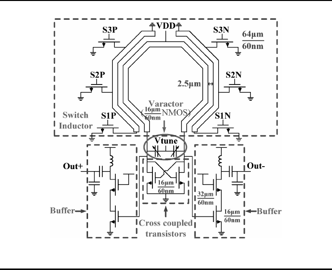
Figure 4.23: Schematic of the 60-GHz inductive-tuning VCO with
symmetric implementation of the proposed new inductor-loaded
transformer.
maximum difference in the effective length on both sides is maintained within
l. Compared with a symmetric implementation, the proposed symmetric imple-
mentation only introduces limited extra number of switches with small FTR
reduction, but can significantly improve phase noise with constraint phase
noise variation. As verified by measurement, this symmetr ical configuration
results in low phase noise with small variation across all sub-bands, while still
maintaining a high FTR.
VCO Design
To verify the proposed symmetric implementation of inductive tuning, an-
other VCO prototyp e is designed at 60 GHz which can also provide multiple
frequency sub-bands to cover the wide frequency band at 60 GHz.
As shown in Figure 4.23, power supply is fed on the central tap. A varacto r-
pair is used for fine tuning within each sub-band. The L C -tank loss is com-
pensated by a cr oss-coupled NMOS pair. Two output buffers are utilized for
the power gain and isolation. The transformer is implemented with the top
metal layer for high Q. Different from the asymmetric implementation, a gap
size of 2.5 µm instead of 3.5 µm is designed between transfor mer primary and
secondary coins . Once the coupling factor of transformer is determined, an

Oscillator 95
Table 4.9: EM Extracted Parameters at 60 GHz for Symmetric
Loaded Transformer Implementation
L
1
(pH) L
2
(pH) M
12
(pH) k
153.1 136.9 44.6 0.308
optimized switch size can be found. Again, a different size of 64 µm/60 nm
is adopted for switch transistors in the symmetric implementation compared
with the size of 50 µm/60 nm in the asymmetric implementation. The size dif-
ferences between two designs come from technology and topology differences,
as we will discuss in Section 4.4.3.2.
With the tuning scheme proposed in Table 4.8, there are 6 sub-bands gen-
erated by the symmetric VCO. Compared to the asymmetric VCO intro duced
in Section 4.4.2 which can provide a wider FTR due to more sub-bands and
fewer loaded s w itches thus smaller parasitic capacitance , the symmetric VCO
significantly improves the phase noise performance with highly suppressed
phase noise variation and can still achieve a wide FTR.
4.4.2.2 Simulation and Measurement Results
The designe d symmetric 60-GHz VCO is implemented in Global Foundries
65-nm CMOS 1P8M technology. EM simulation (ADS-Momentum) is used
for circuit design and verification before the fabrication.
For a fair comparison to the asymmetric 60-GHz VCO presented it Sec-
tion 4.4.2, different transformer and switch sizes are designed for the two
fabrications to a chieve the same primary inductance L
1
as well as equivalent
Q-factors Q
eq
. In this way, similar oscillation frequency as well as similar loss
introduced by loaded transformer can be e nsured. The extracted parameters
for the transformer used for the symmetric VCO are summar ized in Table
4.9, and the equivalent circuit parameters under various band selection modes
are plotted in Figure 4.24. Also note that a square shape is adopted for the
transformer for ease of switch allocation. Though an octagonal shape is theo-
retically less lossy, the effect is minimal for single-loop transformer at 60 GHz
according to simulation.
Phase Noise Analysis
Similar to the a symmetric leaded transformer, percentage of noise contribu-
tion from switches o n loaded transformer to output is simulated and plotted
in Figure 4.29 for symmetric loaded transformers at offset frequencies of 1
MHz a nd 10 MHz. Compared with asymmetric implementation, less noise
contribution is o bserved for symmetric implementation. Although similar Q
eq
values in Figure 4.16 and Figure 4.24 indicate s imilar loss introduced by loaded
transformers, a smaller k value means less noise coupling from switches, which
gives better PN performance at the penalty of smaller FTR. As s uch, one can

96 Design of CMOS Millimeter-Wave and Terahertz Integrated Circuits
Figure 4 .24: Parameter extraction for the symmetric loaded trans-
former design under various band selection modes.
observe 4-dB improvement of average PN performance for symmetric loaded-
transformer design.
Similar to the asymmetric loa de d transformer, the drain-to-source thermal
noise from ”ON” switches dominate the total noise contribution in high fre-
quency bands, while noise contribution from OFF switches not in the current
return path becomes larger at lowe r fre quency bands where a large por tion of
secondary coil is left floating.
Again, the deviation of total switch noise between 1-MHz offset and 10-
MHz offset shows the role of flicker noise from switches. In lower frequency
bands, where a large portion of secondary coil is left floating, a standing wave
would be formed on the floating coil, introducing a large voltage swing at
the floating end, which drives switches into s aturation region. As a result,
more flicke r noise is up-converted and coupled to output. In higher frequency
bands, the floating coil becomes shorter and the contribution of flicker noise
from switches become neg ligible.
Measurement Results
The mea surements are then done on CASCADE Microtech Elite-300 probe
station, with Agilent PNA-X spectrum analyzer, E5052 source signal analyze r,
and 11970V harmonic mixer. Different from asymmetric VCO which requires
a bias-T to provide load to buffer, in this design, the whole buffer is rea lized
on-chip.
The die pho to for the designed symmetric 60-GHz VCO is shown in Figure
4.26. The VCO core occupies an area of 140 × 220 µm
2
. The overall chip size
is 840 × 750 µm
2
, including the test buffer a nd all the pads.
The DC power dissipation of the VCO is 6 mW at supply voltage of 1.0 V.
The lower power consumption compared to asymmetric 60-GHz VCO is due to
the designed high-quality factor of the symmetrical transformer. Figure 4.27
shows the measured tuning curves with dependenc e on the control voltages.
One can obse rve that the VCO can exhibit 6 sub-ba nds with oscillation in

Oscillator 97
Figure 4.25: Percentage of noise contribution from switches on sym-
metric loaded transformer im plementation at 1 MHz offset and 10
MHz offset. Both total noise from all switches and drain-to-source
thermal noise from “on” switches are plotted.
a wide FTR from 57.0 GHz to 65.5 GHz, which covers the whole 60 bands
in IEEE 80 2.15.3c standar d. The tuning range is 8.5 GHz with 14.2% of the
center frequency. The effective K
V CO
in each band varies from 1.8 to 2.4
GHz/V.
Moreover, Figure 4.28 shows the measured phase noise at 10-MHz offset
frequency of the VCO. In the required frequency range (58.32–64.8 0 GHz), the
phase noise at 10MHz frequency offset is lower than -105 dBc/Hz. Both the
mean phase noise (
P N ) and phase noise variation (σ
P N
) has been significantly
improved over the first as ymmetric design due to symmetric tuning adopted,
with σ
P N
improved to -10 8.3 dBc/Hz and σ
P N
reduced to 2.5 dB. Though
the trade-off is reduced FTR, a la rge tuning range of 14.2% is still achieved.
In addition, the measured spectra of the output signals under different
modes are shown in Figure 4.29. The starting frequency under different mode s
distribute evenly as expected, with a small variation from 1 GHz to around
1.6 GHz. Note that this varia tion could be further suppressed by adjusting
switch locations.
The performance of the symmetric VCO prototype is summa rized in Table
4.10 and compared with the asymmetric VCO prototype as well as previously
published 60-GHz VCOs. The asymmetric VCO is able to achieve a very
wide FTR o f 25.8% with the moderate figure-of-merits (FOM and FOM
t
)
defined in ITRS. A large phase noise variation of 8.2 dB is observed because
of asymmetric design. The symmetric VCO shows improved phase noise with
noise variation (σ
P N
) of 2.5 dB achieved in the table with a phase noise mean
(σ
P N
) of -108.3dBc/Hz while a high FTR of 14.2% is still maintained, lea ding
to a state-of-the-art FOM
t
of -179.4 dBc/Hz.

98 Design of CMOS Millimeter-Wave and Terahertz Integrated Circuits
Figure 4.26: Die photo fo r the 60-GHz symmetric VCO fabricated in
Global Found ries 65 nm CMOS technology.
Figure 4.27: Measured tuning curve s under different band selection
modes for the 60-GHz symmetric VCO.
4.4.3 90-GHz VCO Prototype with CRLH T-Line-
Based RTW
The above two VCO prototypes verify the proposed inductive tuning method,
which is applied in tunable CRLH T-line in Section 4.4.1 for RTW VCO
design. To verify the proposed CRLH T-line-based RTW VCO, one 90-GHz
VCO prototype is demonstrated on CMOS 65-nm technology in this section
..................Content has been hidden....................
You can't read the all page of ebook, please click here login for view all page.