

272 Design of CMOS Millimeter-Wave and Terahertz Integrated Circuits
Figure 12.11: Simulation results of the three-stage power gain ampli-
fier with output buffer.
Figure 12.12: Chip micro photograph of the proposed CMOS 280-
GHz heterodyne receiver with on-chip integrated circular polarized
SIW antenna.
directly injected via a waveguide GSG pro be with 50-µm pitch from 220 GHz
to 330 GHz, and a RF signal is emitted by a 20-dB gain ho rn antenna placed
right above the chip under-test by 10-cm distance. The output IF signal is
connected to another low-frequency GSG probe with 100-µm pitch.
The r eceiver output power is measured by a spectrum analyzer (Agilent
E4408b) when the power of the RF source (VDI) is pushed to the maximum
power level (∼ -10 dBm). The receiver gain in (12.4) can be obtained by

CMOS THz Imaging 273
Figure 1 2.13: Equipment setup for 280-GHz receiver measurement.
Figure 12.14: Gain and sensitivity measurement results when sweep-
ing RF and LO frequencies with F
LO
= F
RF
+ 3GHz.
G
tot
(dBi) = P
IF
− ERIP
RF
+ L(d), where P
IF
is the output power of the
receiver in dBm, ERIP is the equivalent isotropically radiated power o f the
signal source in dBm, L(d) is signal propagation loss in dB and d is the
274 Design of CMOS Millimeter-Wave and Terahertz Integrated Circuits
Figure 12.15: Gain measurement results when sweeping RF and LO
frequencies with F
IF
= F
LO
+ 280GHz.
Figure 12.16: Receiver s ensitivity at 250 GHz versus receiver reso lu-
tion bandwidth.

CMOS THz Imaging 275
distance between the horn antenna and the SIW antenna in the receiver. No te
that ERIP
RF
and L(d) can be obtained by the following equations:
(
ERIP
RF
= P
T X
+ G
T X
L(d) = 20 log
c
4π f d
+ 4.343αd
(12.6)
where P
T X
is the source power, G
T X
is the horn antenna gain, and α is the
attenuation factor due to the atmospheric absorption, which is almost negli-
gible for an in door environment. The wide-band gain response is measured
by fixing IF output frequency (f
IF
) at 3GHz and sweeping RF and LO fre-
quencies (f
RF
and f
LO
) simultaneously with f
LO
= f
RF
+ f
IF
. As shown in
Figure 12.14, the pro posed receiver is measured with an operating bandwidth
of 42 GHz from 239 GHz to 281 GHz and a maximum conversion gain of
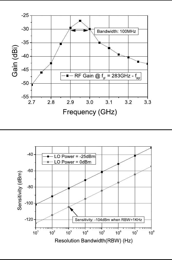
-25 dBi. The narrow-band selectivity response is mea sured by fixing f
LO
at
283GHz and sweeping f
RF
with f
IF
= f
LO
−f
RF
. As shown in Figure 12.15, a
100-MHz r esolution bandwidth is observed. This is slightly lower than the sim-
ulated bandwidth of PGA b ecause of an additional LC resonator in the down-
conversion mixer. The best sensitivity (S) is found to be -31.4 dBm at 250
GHz as illustrated in Figure 12.14, where S is calculated by P SD
noise
·B/ G,
P SD
noise
is the measured output noise power spectrum density from spec-
trum analyzer, B and G are the receiver resolution bandwidth and conversion
gain, respectively. Due to the loss of wave guide and probe (∼15dB) at LO
input, the maximum LO power allowed at the mixe r input is about -25dBm,
which largely affects the receiver performance in terms of conversion gain and
sensitivity. According to the relation between convers ion gain and LO power
illustrated in Figure 12.9(b), the compensated receiver gain is -2 dB when
LO power is increased to 0 dBm. Similarly, the receiver sensitivity in the 0-
dBm LO condition is improved to -54.4 dBm as illustrated in Figure 12.14.
Moreover, the receiver sensitivity can be further improved by introducing off-
chip filters with even smaller resolution bandwidth. For example, as shown in
Figure 12.16, a - 104 dB m sensitivity can be achieved at 250 GHz when the
resolution bandwidth is reduced to 1kHz. Note that the maximum imager data
rate is determined by the integr ation time o f each pixel, and can be derived
from the resolution bandwidth (RBW) based on the selected low pass filtering
response. For example, the integration time of a single RC low pass filter is
0.35/RBW (1/Hz).
The r eceiver performance is s umma rized in Table 12.1 and compared to
other recent state-of-the-art CMOS THz image receivers. For the first time, a
CMOS-based THz image system is demonstrated by the heterodyne receiver
with on-chip integrated circular-polarized SIW antenna. T he proposed re-
ceiver has much smaller detection res olution bandwidth when compared to the
other detection method. Especially when comparing to the super-regenerative-
based r eceiver designs with resonant-type narrow-band detection, the resolu-
tion bandwidth is further increased by 15 times, while the system bandwidth
is improved by 30 times. Moreover, the sensitivity of the proposed receiver

276 Design of CMOS Millimeter-Wave and Terahertz Integrated Circuits
Table 12.1: State-of-the-Art CMOS THz Image Receivers Performance Comparison
Parameters
Unit This Work [32] [230] [259] [90 ] [231]
Technology
— 65-nm
CMOS
130-nm
CMOS
130-nm
CMOS
180-nm SiGe
BiCMOS
65-nm
CMOS
65-nm
CMOS
Freq uency
GHz 239 ∼ 281 280 280 93-113 183 201
Detection
Method
— Heterodyne Diode-
detection
Diod e-
detection
Diod e-
detection
Super-
regenerative
Super-
regenerative
Detection Po-
larization
— Circular Linear Linear Linear Linear Linear
System Band-
width
GHz 42 7 700 20 1.4 1.5
Resolution
Bandwidth
GHz 0.1 7 700 20 1.4 1.5
Gain
dB -25/-2* — 31 39 — —
Sensitivity
dBm -31.4/-54.4* -26.9 — -56 -72.5 -59.6
Power
mW/pixel 6.6 2.5 0.1 225 13.5 18.2
Chip Area
mm
2
/pixel 0.03 3.8 0.25 0.29 0.45 0.99
∗Calculated results when 0-dBm LO power is applied to the mixer.
..................Content has been hidden....................
You can't read the all page of ebook, please click here login for view all page.