
B.5. Output Characteristics of BJT in the Common-Emitter Mode
The common-emitter terminal configuration can be considered the fundamental building block of BJT analog amplifier circuits. The common base and common collector are applied to some extent in more special-purpose roles, such as for high output resistance (common base) and low output resistance (common collector). Therefore, a study of the transistor in the common-emitter mode is basic to a study of analog circuits.
The output characteristic of the common-emitter transistor is defined as the output current (IC) as a function of the output terminal voltage (VCE) for IB (or VBE) held constant. It is very important to understand in the design of both analog and digital circuits. The output characteristic is experimentally explored in the project on parameter determination. The measurement circuit for obtaining the output characteristic is shown in Fig. B.12. This is also the circuit for measuring βDC versus IC, which is discussed below.
Figure B.12. Circuit for measuring transistor output characteristic and βDC versus IC.

The equations presented in Unit B.2 are in terms of terminal voltages VBE and VBC. The common-emitter configuration has input voltage VBE but output voltage VCE. Therefore, it is preferable to eliminate VBC in the equations in favor of VCE, using VBC = VBE – VCE.
When plotting the output characteristic, for example, from 0 < VCE < 5 V, the range of VBC is VBE < VBC < –(5 – VBE). Since VBE ≈ 0.5 V, VBC covers the full range from strongly forward biased (out of the forward-active mode) to clearly reverse biased (forward-active mode). This requires that the IC [(B.7)] and IB [(B.12)] equations be modified to include all possibilities.
To obtain an equation for IC under general biasing conditions, we start with the fundamental equation of transistor action of the BJT. This is
Equation B.20

This is a composite of (B.7) and (B.13) in which the base-modulation effects are neglected. Both of these equations are for IC and IE in the ideal transistor. (In this unit and beyond, we assume that nF = 1.) Sometimes referred to as the linking-current equation, this is symmetrical in IC and IE and neglects all components of base current and dependence of the base width on VBC and VBE.
To add an additional degree of applicability to the real transistor, base-width modulation must be added. We are interested in a relation between currents and voltages for the transistor in the forward-active mode. In this case, VBE is fixed at 0.4 < VBE < 0.6 V. On this basis, base-width modulation of the emitter – base junction can be neglected. On the other hand, the relation must apply for a VBC range, which includes relatively large negative values. Therefore, the effect of base-width modulation of the collector – base junction must be included in a modification of (B.20). If base-width modulation due to the dependence of base width on VBC is added and the substitution VBC = VBE – VCE is now made, (B.20) becomes:
Equation B.21

The general equation must include any significant base current that contributes to collector current, that is, for when the base – collector junction becomes forward biased. For this we use (B.14) with base leakage current neglected. (Leakage current is neglected throughout this unit.) This is
Equation B.22

The –1 term has been retained in order for the equation to apply at all possible polarities and values for VBC = VBE – VCE, including zero where this contribution of collector current is zero.
We note that this base current is in a loop (Fig. B.8) through the base – collector junction and is positive out of the collector terminal; IC of (B.21) is positive into the collector terminal as in Fig. B.7. Thus, the component of base current from (B.22) subtracts from the collector current to give
Equation B.23
![]()
Again, for simplicity, this equation neglects the leakage current associated with the collector – base junction [ISC term (B.14)], which is only a fair approximation for the level of IC at which we will obtain an output characteristic in the parameter extraction project on the BJT.
A plot of this equation for IC as a function of VCE can be obtained for constant VBE or constant IB. For the latter, VBE is also a variable such that the plot requires, in addition, a solution for VBE as a function of VCE for constant IB. In the project on the output characteristic, the measured data and a SPICE solution are compared during the measurement. The input circuit provides a more or less constant IB. However, the SPICE solution, which is computed by LabVIEW, is exact. It allows for a variable IB and associated variable VBE. The SPICE solution formulation used by LabVIEW is outlined below in Unit B.7. The SPICE solution is also explored in the project Mathcad file.
After measuring the output characteristic, the segment of the resulting data array from the active region (VCE > VBE) is extracted. From these data, a straight-line curve fit is obtained by LabVIEW, which produces a number for the slope. From (B.23), we obtain an equation for the active region from letting VCE > VBE, with the result
Equation B.24
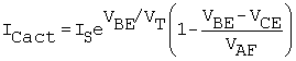
The slope for the active-region equation is slope = dICact/dVCE = IC/VAF. Thus, VAF can be calculated from VAF = IC/slope, where IC is the value taken from the data array for VCE = VBE.
For the special case of VCE = VBE, one can obtain a value for IS from the relation
Equation B.25

After VAF and IS have been obtained, an iteration on βR will produce a final curve fit to the output characteristic, thereby providing a number for βR. In this manner, all three parameters of this unit are obtained: IS, βR, and VAF.
An example of a SPICE output characteristic (calculated in Mathcad), which uses the measured transistor-model parameters, is shown in Fig. B.13. Also shown is the calculated active-region plot.
Figure B.13. Mathcad calculated plot of the complete output characteristic, (B.23), and the active-region segment, (B.24). The saturation region [(B.34)] is graphically revealed where the plots separate.

The low-voltage region where IC < ICsat is called the saturation region. The voltage and current in this region are VCEsat and ICsat. In the derivation of the general equation for IC, (B.23), the leakage current of the base – collector junction was neglected. If this is not valid, the reverse βR, which is determined through curve fitting, is somewhat artificial. For example, suppose that the leakage current totally dominates the collector – base current. For this case, the general IC equation is
Equation B.26

where a new definition of a sort of βR is defined in the relation ISC = IS/βRleak. A curve fit to the measured output characteristic would give βRleak. However, because nC > 1, the result depends on the level of collector current at which the measurement is made. If, in a given measurement, the βRleak is interpreted as βR, it would function as βR in SPICE (when assigning BR to the model), but it would only be valid in a simulation for collector currents close to that of the measurement.