
2.1. BJT and MOSFET Schematic Symbols, Terminal Voltages, and Branch Currents
The BJT can be either a pnp or an npn. The MOSFET similarly can be a pmos or an nmos. The equivalents are npn and nmos and pnp and pmos. The following discussion is based on the npn and nmos, as shown in Fig. 2.1. (All polarities and current directions are reversed for the pnp and pmos. This provides for important versatility in applications.)
Figure 2.1. BJT npn and MOSFET nmos transistors. The terminal configurations are designated common emitter and common source.
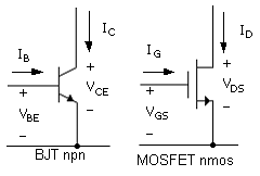
The BJT terminals are designated collector, base, and emitter while those of the MOSFET are drain, gate, and source. The terminal configurations in Fig. 2.1 are, for the BJT, the common emitter, and for the MOSFET, the common source, in amplifier-stage parlance. This suggests that both the input (left side) and output (right side) are referred to the common terminal. For example, for the BJT, the input terminal voltage is VBE and the output terminal voltage is VCE. Similarly, for the MOSFET, we have VGS and VDS. Note that in the convention of subscripts in electronics, the first subscript is assigned positive. This matches the assignments in the diagram, and the plus and minus signs are superfluous.
Note also the convention for symbols for all currents and voltage.
Total voltage and current: vXY, iX
Dc, bias, quiescent, or operating point: VXY, IX
Signal or ac (RMS, peak): Vxy, Ix
General instantaneous signal: vx, ix
The voltage and current symbols in Fig. 2.4 are therefore for dc. For a voltage, a single subscript means that this terminal (or node) voltage is referred to the common terminal. For example, in the npn case above, VCE = VC.
Figure 2.4. Basic NMOS amplifier with resistor gate biasing and input signal Vs. (a) Complete circuit. (b) Signal (or ac or incremental) circuit. The signal circuit is obtained by setting the power supply (dc) node to zero volts. (c) Linear signal circuit replaces the linear schematic representation.

The input terminals vBE and vGS are the control terminals; that is, they control the output currents iC and iD. In both cases, the terminal pairs possess extremely nonsymmetrical voltage – current behavior. With the polarities as shown, the currents flow readily, whereas with the opposite polarities, the output currents are cut off or are, for most purposes, essentially zero.
The basic (simplified) general relations between the currents and voltages are:
Equation 2.1
![]()
Equation 2.2
![]()
IS, VT, kn, Vtn, and VT are device model parameters or physical constants.
In linear circuit applications, for example, as amplifier stages, the transistors are provided with a circuit configuration that sets up dc, or bias, currents and terminal voltages (sometimes referred to as the Q-point, for quiescent, or in SPICE, the operating point). In the amplifier application, a signal voltage is applied to the input, that is, superimposed on the dc magnitude, which must be much smaller than the dc voltage if the signal input-output relation is to be linear. This is apparent from (2.1) and (2.2), which are nonlinear relations. All of the currents and terminal voltages will change in response to the input signal, and all of these incremental changes must be small compared to any of the dc currents or voltages, in order for the linear relationships to be valid.
In circuit applications, both types of transistors are operated in all three possible terminal configurations. This provides for a wide variety of amplifier-stage characteristics, including gain and input and output impedance.