
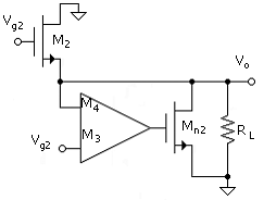
14.8. Output Circuit of the TS271 Opamp
The TS271 operational amplifier is designed to operate at very low current levels. This would include the current of the source follower of the output stage. In this case, the output resistance of an amplifier with a simple source-follower stage for an output stage, such as in Fig. 14.7, would be unacceptably high. In the TS271 operational amplifier, the 9-transistor circuit of Fig. 14.8 replaces the simple source-follower stage consisting of M6 and M13 of Fig. 14.7. Note that the circuit of Fig. 14.8 uses different transistor designators. In Fig. 14.7, M6 and M13 are equivalent to M1 and Mn1 of Fig. 14.8.
Figure 14.8. The output stage of the TS271 opamp. The new source follower consisting of M1 and Mn1 is equivalent to the stage of M6 and M13 of the amplifier of Fig. 14.7.

The circuit of Fig. 14.8 has an additional source-follower stage consisting of M2 and Mn2. The output from the common-source stage (drain of M3 of Fig. 14.7) is applied to the gates of both source-follower stages. The sources (outputs) of M1 and M2 are connected to the inputs of the differential-stage gates of M3 and M4, respectively. There is no load at the source of M1 such that the gain of the source follower can be considered unity. Thus, Vg3 ≈ Vg2 = Vg1 (incremental voltages). By contrast, the source of M2 is connected to RL such that, in general, Vo = Vs2 < Vg2.
From another perspective, suppose Vg2 = 1V, that is the source-follower gates are raised by 1V above the bias level. With a load, RL, the current increase will be greater for M2 compared to M1. This will cause the source voltage of M2 to be slightly lower (than that of M1) such that the input to the differential amplifier is nonzero and the output voltage (drain of M3) will drop. The result is a reduction of the gate voltage of Mn2 and thus a reduction of the drain current in Mn2. The incremental drain current of Mn2 provides most of the current through the load; the load current is dominated by the change in the current of Mn2 instead of M2.
Fig. 14.9 is a reasonable equivalent, incremental, circuit. The differential stage (M3, minus, M4, plus, and the drain of M3 as the output) is represented by an opamp symbol.
Figure 14.9. Equivalent circuit of the output stage of Fig. 14.8. The opamp symbol represents the differential-amplifier stage of M3 and M4.
Since the source follower of M1 has a transfer function of nearly unity, incremental Vg2(= Vg1) is moved directly to gate of M3 (minus input of the differential amplifier) as in Fig. 14.9. Thus
Equation 14.39
![]()
where avda is the gain of the opamp and the output of the opamp is Vgsn2. The amplifier (output stage) output voltage is therefore
Equation 14.40
![]()
where we now assume that gm2 = gmn2. It follows that the relation between Vgs2 and Vo is
Equation 14.41
![]()
Combining this with
Equation 14.42
![]()
gives the transfer function, input to output, as
Equation 14.43
![]()
where
Equation 14.44
![]()
The output resistance of the circuit of Fig. 14.8 is 1/Gm. The output resistance of the circuit of Fig. 14.8 is thus reduced by a factor of about 1/avda compared to the circuit of Fig. 14.7 for the same gm of the source follower transistors. From (14.18), the gain of the differential-amplifier stage is
![]()
This would typically be on the order of 100. Thus a significant benefit over the simple source-follower stage output is realized with the circuit of Fig. 14.8. It is also significant that there is no body effect associated with Mn2.