
3.2. Output and Transfer Characteristics of the MOSFET
The equations used in the following to characterize the MOSFET transistor are from the SPICE Level 1 model. SPICE also has more detailed models in Level 2 and Level 3. These can be specified when running SPICE. However, the number of new model parameters, in general, in circuit simulation is practically boundless. Level 1 is chosen here as it is the most intuitive, that is, the most suitable for an introductory discussion of device behavior. Some new models, for example, which focus on frequency response at very high frequencies, can include pages of equations. In addition, Level 1 is suitable and adequate for many examples of circuit simulation.
The basic common-source NMOS circuit configuration is repeated in Fig. 3.2. Here it serves as a basis for discussing the dc SPICE parameters of the MOSFET transistor. In the example, VDS = VDD. The output characteristic is a plot of ID versus VDS for VGS = const. A representative example is shown in Fig. 3.3. As mentioned, the low-voltage region is referred to as the linear region, triode region, or presaturation region. Outside this region for higher voltages is the active (saturation) region. This is referred to here as the active region to avoid confusion with the fact that the nomenclature is just the opposite in the case of the BJT; that is, the low-voltage region is called the saturation region. As discussed in Unit 3.1, the linear and active regions are delineated by Veffn ≡ VDSsat = VGS – Vtno.
Figure 3.2. Common-source circuit configuration for discussion of the dc model parameters of the NMOS transistor. The three-terminal transistor symbol implies that the body and source are connected.
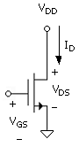
Figure 3.3. Mathcad-generated output characteristic for the NMOS transistor. The plot illustrates the linear and active regions. The linear region is also called the triode region or presaturation region. Current is in microamperes and Veffn = 0.8 V. Also plotted is the ideal characteristic with zero slope in the active region.

The output-characteristic equation in the linear region corresponds to VDS ranging from the condition of Fig. 3.1(b) to that of Fig. 3.1(c). As VDS increases from zero, the channel begins to close off at the drain end (i.e., the channel becomes progressively more wedge shaped). The result is an increase in the resistance of the channel as a function of VDS, and therefore a sublinear current – voltage relation develops.
When VGS > Vtno, the electron charge in the channel can be related to the gate voltage by Qchan = Cox(VGS – Vtno) (per unit area of MOSFET looking down at the gate), where Cox is the parallel-plate capacitance (per unit area) formed by the MOS structure. This provides a simple linear relation between the gate voltage and the charge in the channel.
The conductivity in the channel is σchan = μnQchan/tchan, where μn is the mobility of the electrons in the channel and tchan is the thickness of the channel into the semiconductor. Thus, in the case of a uniform channel (i.e., for VDS → 0), the channel conductance is
Equation 3.2
![]()
where
Equation 3.3
![]()
and where KPn = μnCox is the SPICE transconductance parameter (the n subscript is the equation symbolic notation for the NMOS; the parameter in the device model is just KP), W is the physical gate width, and L, again, is the channel length. Parameter KPn is related to the electron mobility in the channel and the oxide thickness. Therefore, it is very specific to a given MOSFET device.
As VDS increases, but is less than Veffn [transition from Fig. 3.1(b) to 3.1(c)], the wedge-shaped effect on the channel is reflected functionally in the channel conductance relation as
Equation 3.4
![]()
This leads to an output characteristic equation for the linear region, which is
Equation 3.5
![]()
The derivation leading to (3.4) and (3.5) is given in Unit 3.4. The linear-region relation, (3.5), is applicable for VDS up to VDS = Veffn, which is the boundary of the linear and active regions. The active-region equation is then obtained by substituting into (3.5), VDS = Veffn, giving
Equation 3.6
![]()
This active-region current corresponds to the zero-slope ideal curve in Fig. 3.3. As discussed in Unit 3.1, the drain current is not actually constant in the active region (in the same manner as for a BJT), due to the fact that the physical length of the channel is reduced for increasing VDS beyond VDS = Veffn. The reduction in the channel length has the effect of slightly reducing the resistance of the channel. This is taken into account using the fact that kn ∝ 1/L, from (3.3), where L is the effective physical length between the source and drain regions. For VDS > Veffn, a reduced length L′ = L(1 – λnVDS) is defined which leads to a new effective ![]() ,
,
Equation 3.7
![]()
where λn is the SPICE channel-length modulation parameter (Lambda). Substituting ![]() for kn in (3.6) produces
for kn in (3.6) produces
Equation 3.8
![]()
(Note: A preferred form would be ID = kn Veffn2[1 + λn (VDS – Veffn)] because the channel-length effect only begins for VDS > Veffn and kn could be defined properly for effective length L at VDS = Veffn. Level 1 SPICE uses (3.8).)
Level 1 SPICE also applies this channel-length reduction factor to the equation in the linear region, (3.5). To match the linear-region equation to the active-region equation, (3.5) becomes, at the edge of the active – linear regions,
Equation 3.9
![]()
and, in general
Equation 3.10
![]()
[Again, the fact that the channel length is not reduced with the transistor in the linear region would suggest the use of (3.9) throughout the linear region. Level 1 SPICE uses (3.8) and (3.10).]
In general, Vtn is a function of the source-body voltage, VSB. We assume for the moment that VSB = 0. This applies, for example, to the common-source circuit in Fig. 3.2, since the body will always be at zero volts, and the source in this case is grounded as well. For this case, Vtn = Vtno, as used above. In laboratory projects we measure the output characteristic from which parameter λn can be obtained. This is based on (3.8). The I – V slope in the active region is
Equation 3.11
![]()
From the data measured, a straight-line curve fit determines the slope and the zero VDS intercept (ID at VDS = 0). These are used in (3.11) to obtain λn from λn = slope/intercept. The intercept is the extension of the active region of Fig. 3.3 (dashed line) to the ID axis.
When applying the equations of this development to the PMOS, the voltage between the gate and source is defined as positive with respect to the source, that is, VSG. To be consistent, the threshold voltage for the PMOS, Vtp, is also positive. In the SPICE model, however, the threshold voltage is assigned negative because positive is taken for both types of devices with respect to the gate (VGS is negative for the PMOS), and the threshold voltage for the PMOS is negative.
The transfer characteristic is obtained by holding VDS constant and varying VGS. In the MOSFET parameter-determination experiments of Projects 3 and 4, we plot VGS versus ![]() for the transistor biased into the active region. The equation is
for the transistor biased into the active region. The equation is
Equation 3.12
![]()
where ![]() is (3.7)
is (3.7)
![]()
The slope in (3.12) is ![]() and the zero
and the zero ![]() intercept is expected to be Vtno. LabVIEW obtains the slope and intercept from a straight-line fit to the data. The measured transfer characteristic thus yields the two parameters
intercept is expected to be Vtno. LabVIEW obtains the slope and intercept from a straight-line fit to the data. The measured transfer characteristic thus yields the two parameters ![]() and Vtno.
and Vtno.
In Project 4, parameter λn is obtained from finding ![]() at two different VDS values. This is based on
at two different VDS values. This is based on
Equation 3.13
![]()
where the ![]() values are measured and λn is the only unknown.
values are measured and λn is the only unknown.