
3.3. Body Effect and Threshold Voltage
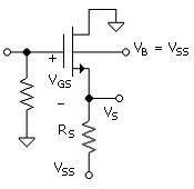
In Fig. 3.4 is shown an example of a circuit in which the body and source cannot be at the same voltage. We now use the four-terminal symbol for the NMOS, which includes the body contact. In most applications, the body would be tied to the lowest potential in the circuit (NMOS), in this case, VSS (e.g., VSS = –5 V). But by the nature of the circuit, the source voltage is VS = VSS + IDRS, such that the source-body voltage is VSB = IDRS.
Figure 3.4. NMOS transistor circuit with a resistor, RS, in the source branch. With the body attached to VSS, VSB = IDRS.
In MOSFET devices, the threshold voltage depends on VSB and in SPICE is modeled according to (NMOS)
Equation 3.14
![]()
SPICE parameters contained in the equation are Vtno (VTO), γn (Gamma), and 2ΦF (Phi) (Table 3.1). Typically, γn ≈ 0.5 V1/2 and 2ΦF ≈ 0.6 V. Therefore, for example, for VSB = 5 V, the body effect adds 0.8 V to Vtno.
In the case of the CMOS array ICs of our lab projects (CD4007), the body effect for the PMOS is significantly less pronounced than for the NMOS (γp < γn), but the parameter for the channel-length-modulation effect is much smaller for the NMOS than for the PMOS (λn < λp). The combination suggests that the chip is a p-well configuration; that is, the NMOS devices are fabricated in “wells” of p-type semiconductor that are fabricated into an n-type substrate. The PMOS devices reside directly in the n-type substrate material. As far as our measurements are concerned, the extremes in parameters are an advantage, as we are interested in observing the effects of the various parameters.
In Project 4, a number for γn is obtained by measuring Vtn as a function of VSB. The results are plotted as Vtn versus ![]() . LabVIEW calculates the X variable. The data plotted should give a straight line with slope γn. The effectiveness of SPICE modeling for representing the behavior of the transistor in a circuit is investigated in Project 4. The transfer characteristic, VGS versus ID, is measured for a circuit of the type shown in Fig. 3.4, where the circuit has VSB = IDRS. In the project, VSS is swept over a range of values to produce a range of ID of about a decade. From (3.14), the threshold voltage characteristic that includes the body effect is
. LabVIEW calculates the X variable. The data plotted should give a straight line with slope γn. The effectiveness of SPICE modeling for representing the behavior of the transistor in a circuit is investigated in Project 4. The transfer characteristic, VGS versus ID, is measured for a circuit of the type shown in Fig. 3.4, where the circuit has VSB = IDRS. In the project, VSS is swept over a range of values to produce a range of ID of about a decade. From (3.14), the threshold voltage characteristic that includes the body effect is
Equation 3.15
![]()
The input circuit loop equation (Fig. 3.4) is
Equation 3.16
![]()
Including the body effect, VGS is now [from (3.12)]
Equation 3.17
![]()
where, for this special case, VDS = VGS (VD = 0, VS = 0).
A solution is obtainable through combing (3.14), (3.16), and (3.17) for ID and VGS. These equations contain every parameter from this discussion of MOSFET SPICE parameters along with RS. In a project Mathcad file, Project04.mcd, a solution is obtained to provide a comparison with the measured VGS versus ID for the circuit. The Mathcad iteration formulation is, from (3.16),
Equation 3.18
![]()
Equation 3.19
![]()
ID and VGS are found for the range of VSS corresponding to that used in the measurement, which is 2.5 < |VSS| < 10 V.