
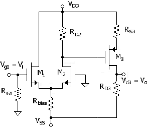
13.3. Stabilization of Signal Gain and Bias Current with a Source Resistor
The amplifier of Fig. 13.1 is not a good design in terms of bias stability. Bias current ID3 (of M3) in the circuit of Fig. 13.1 is very sensitive to the voltage across RD2, which, in a relative sense, is only marginally predictable, given the normal variation in device parameters and circuit components. Also, as in the bias-stability discussion of Unit 5.5 on the design of the NMOS common-source amplifier, for a constant VGS3, bias current ID3 is sensistive to changes in transitor parameters. (Note that the differential-amplifier-stage bias current is relatvely stable, as it is a current-source bias current.)
13.3.1. Gain and Gain Stabilization
As noted, it was shown in Unit 5.5 that a degree of bias stability is provided with a source resistor as in the circuit of Fig. 13.2 (in this case, RS3). This is an additional example of providing some stabilization with the addition of ac and dc negative feedback in a circuit. The addition of the resistor results in an increase in the gain of the differential amplifier stage but a decrease in the gain of the common-source stage. The net result is a reduction of gain as a trade-off between the gain and bias stability.
Figure 13.2. Amplifier circuit with the addition of a source resistor, RS3, which serves to improve the gain and bias stability. This again demonstrates a general principle, often used in electronic circuits, wherein a linear component is installed to dominate the voltage of voltages in series.
The gain expression for the circuit with RS3 is
Equation 13.4
![]()
where (5.15) is now used for the gain of the common-source stage. It is useful again to express the result in terms of Veffn and Veffp and the voltages across resistors to make a quantitative assessment of the gain. Using gm = 2ID/Veff [(4.5)], the gain expression is
Equation 13.5
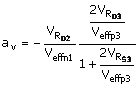
For example, we set VRS3 = 1 V, with a new VRD2 = 2.3 V. The gain magnitude is now |av| = 7.67 · 4.35 = 33.3, compared with 116 for the circuit of Fig. 13.1. Note that the contribution from the differential stage increases from 4.3 to 7.7.
The output-resistance effect on the gain of the common-source stage is neglected [as in (5.15]. This is justified as the output resistance at the drain of M3 is increased significantly with RS3. [Precision gain equation (8.34) gives 4.21 compared with 4.35 using (5.15)]. This is discussed further below in conjunction with the common-source amplifier with source resistor from the viewpoint of a feedback circuit.
If resistor VRS3 is sufficiently large, gm3RS3 >> 1. In this limit the gain is
Equation 13.6
![]()
The magnitude of gain given by (13.6) is about 38, a fair approximation to the value of 33 from (13.5). It is apparent from the form of (13.6) that a significant degree of gain stabilization has been achieved, as the gain depends primarily only on the bias currents ID1 = ID2, which is quite stable in the differential amplifier circuit.
13.3.2. Transistor Parameter Variation and ID3 Bias Stability
The benefit to ID3 bias stability associated with transistor parameter variation can be assessed by a consideration of (5.18) applied to this case, which is

For a quantitative example, suppose that ID3 = 100 μA. To be consistent with the numbers used in Unit 13.2, kp3 = 1110 μA/V2 with Veffp3 = 0.3 V.
Assume that VRD2 = ID2RD2 is constant. Now make kp3 5% larger and Vtpo3 50 mV smaller. For the VRD2 = 2.3 V, we have a new ID3 = 105 μA for VD3 = 0.25 V, which is an acceptable bias value. For the circuit of Fig. 13.1, and the same parameter changes, the new bias current is ID3 = 143 μA for VD3 = 2.15 V, significantly away from the design zero volts.
13.3.3. Bias Stability of ID3 Due to Changes in ID2
The actual differential-stage bias current will vary from the basic design due to the variation in circuit components, transistor parameters, and power-supply voltage. Suppose that in lieu of the value of VRD2 = 2.3 V as in the example above, VRD2 is 5% higher or 2.42 V. Assume that the transistor parameters of the common-source stage are at the original design values.
An estimate of the new output voltage (different from 0V) can be made using the linear relation between the input and output of the common-source stage, that is, the common-source contribution of (13.4). The “signal” is the change of voltage across RD2, which is –0.12 V. (The gate voltage vG3 decreases.) The common-source gain from (13.4) for the original parameters associated with M3 is –4.35. The output bias voltage is now (–4.35)(–0.12V) = 0.5 V (instead of 0 V). Therefore, the circuit is reasonably bias stable.
The gain of the unstabilized circuit of Fig. 13.1 is –27, which leads to an output voltage, for the same change of voltage across RD2, of 3.2 V, using the linear approximation. Note that the linear approximation is marginally valid only for such a large value of the common-source input “signal” voltage, as in this case of no source resistor. (A dc calculation gives a bias output voltage of 4.8 V.)