
6.2. Current-Source Bias Amplifier: Bypass Capacitor
The PMOS common-source amplifier circuit with the bypass capacitor is shown in Fig. 6.2. At some low frequency, the effect of the capacitor is absent, and the gain is computed from (5.15), which is
![]()
Figure 6.2. Dual-power-supply common-source amplifier stage with bypass capacitor. The object is to determine the frequency for which the source is effectively at signal ground.

Over a range of frequencies, the gain evolves from (5.15) to (5.2), av = –gmRD (neglecting the output resistance of the PMOS). The frequency-dependent transition region is determined by replacing RS in (5.15) with the impedance of RS in parallel with the reactance of Cs. This is
Equation 6.3

or
Equation 6.4

with
Equation 6.5
![]()
and
Equation 6.6
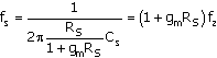
Note that the “RC” factor has an “R,” which is RS in parallel with 1/gm, the latter being the output resistance looking into the source of the transistor. The two frequencies fs and fz are technically the pole and zero of the response function.
We note that gmRS = 2IDRS/Veffp. Since Veffp could be as low as Veffp ≈ 0.2 V, then gmRS >> 1 in some cases. The corner frequency, f3dB, occurs at
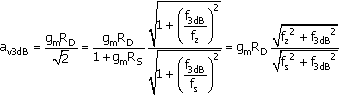
Equation 6.7
which gives
Equation 6.8
![]()
such that
Equation 6.9

where the far-right-hand term applies for gmRS >> 1. This is typically only marginally satisfied in MOSFET circuits.
The derivation carried out here was initiated from (5.15), which neglects the output resistance of the transistor. In the case of the MOSFET devices of our projects, the simplification is valid for the NMOS transistor but marginal for the PMOS transistor. This is because λp >> λn. The result (6.9) still serves to estimate the required value for Cs, even for the case of the PMOS. Nevertheless, a more detailed derivation is carried out in the next unit. This permits comparisons, in a project, of SPICE and Mathcad solutions with amplifier gains and frequency response.