
1.1. Resistor Voltage Divider and MOSFET DC Gate Voltage
Figure 1.1(a) shows a basic NMOS amplifier stage. This is the dc (or bias) portion of the circuit, which excludes the signal part. The terminals of the transistor are designed G (gate), D (drain) and S (source). The design calls for a dc voltage VG, with respect to the zero reference voltage, which is obtained by dividing the supply voltage VDD between bias resistors RG1 and RG2. Since the gate terminal has zero current, the voltage, VG, at the gate can be assessed with the resistor network separated from the circuit as in Fig. 1.1(b). The goal is to relate the node voltage VG to the values of RG1 and RG2 and VDD. The result is the basic resistor voltage-divider relation.
Figure 1.1. (a) Dc circuit for the basic NMOS amplifier. (b) Circuit for determining the gate voltage, VG.

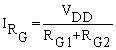
Note that since VDD is given with respect to the reference zero volts, the VDD designation at the top node is equivalent to the supply voltage, also referred to as VDD. The current IRG is
Equation 1.1
The voltage across the resistor RG2 is VG (since VG is with respect to the zero reference) and this is
Equation 1.2
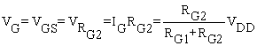
It can be concluded that the gate voltage is the value of RG2 divided by the sum of the two gate-bias resistors.