
14.2. Current-Source Output Resistance and Common-Mode Gain
As discussed in Unit 8, the common-mode gain is the gain for the same signal being applied to both inputs. In Unit 8.6 the common-mode voltage gain expression, (8.26), was obtained for the bias resistor, Rbias. This is
![]()
To apply the common-mode gain equation to the circuit of Fig. 14.1, resistor Rbias is replaced by rds11. The result for the common-mode gain is
Equation 14.2
![]()
The approximate form is consistent with neglecting the change of the gate – source voltage compared to the change of voltage at the drain of the current-source transistor, M11. Intuitively, (14.2) indicates that for rds11 → ∞, transistor M11, is a pure current source, and iD1 = iD2 = ID1 = ID2 regardless of the magnitude of common voltage applied to both gates. In this case, signals Id1 = Id2 = 0 for any (realistic) common-mode input signal.
Common-mode inputs can be a form of noise, and therefore the ideal opamp would reject these signals entirely. An important consideration is the extent of rejection based on the common-mode gain relative to the differential amplifier gain. This is quantitatively assessed with the common-mode rejection ratio, which is the ratio of the differential amplifier gain with differential output divided by the common-mode gain, (14.2). The gain for this case was obtained in Unit 8.5 as (8.24), which is avd12 = –gmRD.
Using (8.24) and (14.2), the common-mode rejection ratio is
Equation 14.3
![]()
With gm1 = 2ID1/Veffn1 [(4.5)], and for the output resistance of M11, rds11 ≈ 1/λn2ID1 [(4.15)], the common-mode rejection ratio is
Equation 14.4
![]()
By comparison, for resistor bias, the equivalent result is
Equation 14.5
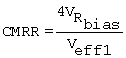
where Rbias is the bias resistor of, for example, the circuits of Figs. 13.1 and 13.2.