P1.5. Frequency Response of a Resistor-Capacitor Circuit
Components
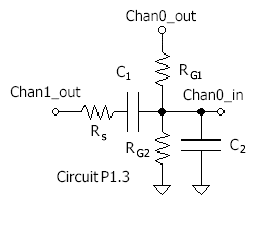
C1 = C2
f3dBhi = 50f3dBlo
Rs ≈ RG/50
f3dBlo = 5 Hz (approximately)
Typical C1 ≈ 0.5 μF
Procedure
Configure the circuit for the low-end measurement and f3dBlo. Install C1 and do not install C2. Run VI_05.vi to obtain f3dBlo. Obtain a Log of the Front Panel to save the results. To obtain a Log, go through menu sequence Operate>>Data Logging>>Log. To retrieve data: Operate>>Data Logging>>Retrieve.
An example of retrieving a Log using VI_01.vi is shown here. Note that at the first Data Logging, you will be asked to name a Data Log file. Select any name and Click Save, to install Log File in the Project folder.
Now move the capacitor C2 = C1 to the C2 location and install a large capacitor, C1new, in place of C1, which satisfies C1new >> C2 (e.g., C1new = 47 μF). Note that the source side of the capacitor (connected to Rs) is more negative than the output side (Chan0_in). Run VI_05.vi to obtain f3dBhi. Default and save the Front Panel. Note that when reopening the VI, the Front Panel will contain the information last defaulted from this f3dBhi measurement. The first measurement is in the data Log. Repeating, to retrieve the information from the data Log, go through menu sequence Operate>>Data Logging>>Retrieve. To then go back to the defaulted Front Panel, click OK and go through Operate>>Reinitialize All to Default Values.
Note that if C2 = C1 are actually both in the circuit at the same time, the output in the plateau region is 1/2 as large (Exercise 1). This configuration is not implemented here. The use of C2 = C1 is only for convenience and f3dBlo << f3dBhi is satisfied with Rs << RG.