
C.1. DC (Bias) Analysis
The two common-emitter amplifier-stage configurations studied in projects are shown in Fig. C.1. We note that the dc circuit of Fig. C.1(a) is that of Fig. B.12. Amplifier performance analysis can be performed with the two output channels available from the DAQ in the following manner: Fig. C.1(a) uses separate channels for the input and output bias circuits and superimposes the input signal on the input bias. In Fig. C.1(b) we add a signal-source resistor and coupling capacitor and use one channel for the input signal and one channel for bias. The capacitor is required to prevent the connection of the signal source from affecting the dc (bias) operation of the circuit. The latter represents the classical practical common-emitter amplifier stage. The signal-source resistor provides for a current-source input signal and hence linear amplification.
Figure C.1. (a) Base current bias (dc) and input signal applied to the same node. Collector circuit has a separate power supply. (b) Amplifier with signal coupling capacitor and single power supply for bias.
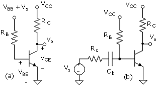
In the experimental project on the common-emitter amplifiers, we measure the voltage gain as a function of the collector current and compare the results with SPICE. The bias collector current is swept from 0.1 to 1 mA. The measurement uses the circuit in Fig. C.1(a). A DAQ output channel (VBB) sets the bias currents. Another output channel (VCC) sets the design bias VCE at each bias current. The gain of the circuit of Fig. C.1(b) is also measured with particular emphasis on the bias solution and the frequency response.
C.1.1. DC (bias) Formulation
A formulation for obtaining the collector current for a given VBB [Fig. C.1(a)] is based on the following: From the input loop equation,
Equation C.1
![]()
The two relevant transistor characterization equations are (B.6),
![]()
and base – emitter dc voltage equation, from (B.7), setting VBC = 0 for simplicity,
Equation C.2
![]()
The equation set above has three unknowns, IC, IB, and VBE. The equations can be combined to obtain a function for IC,
Equation C.3

A good estimate can be obtained with using VBE ≈ 0.6 V, giving simply
Equation C.4
![]()
The simple expression is sufficient, for example, for selecting a value for RB in the circuit of Fig. C.1(a) in the BJT amplifier project. We have also neglected the dependence of βDC on VBC of (B.11). This is a reasonable approximation for establishing the nominal values for the measurement circuit components.
The collector – emitter voltage, VCE, is then established with
Equation C.5
![]()
In designing a project circuit for a current sweep, RB and RC are selected for the highest currents and highest DAQ output voltage. In the amplifier project, the circuit of Fig. C.1(b) uses the resistors from the circuit of Fig. C.1(a). It thus has a unique bias variable and VCC solution for a given design VCE requirement. This is based on (C.3) and (C.5) and is
Equation C.6
![]()
In the amplifier project, the project Mathcad file is used to find the solution for VCC [with an educated guess for VBE, as in (C.4)]. If the result has VCC > 10 V, the limit from the DAQ, it is necessary to decrease RC or increase RB. This may be necessary, as the transistor βDC is not known with precision at the point of the selection of the resistor values. After measuring the actual VCC, the result is used in the Mathcad file to compute a value for βDC from a circuit solution.