
B.3. BJT Base, Emitter, and Collector Currents in the Active Mode
The discussion of the transistor mechanism of Unit B.1 is extended here to include base-current mechanisms, which exist in the real transistor, and the effect of base-width modulation as discussed in Unit B.2. Initially, the case of active-mode operation is discussed, and this is followed by the general-bias case, which includes the possibility of both pn junctions becoming forward biased.
In the device model for the bipolar junction transistor, the parameter βDC is
Equation B.6
![]()
where IB is the composite of all contributions to the base current. (The use of “dc” is consistent with SPICE.) This relates the output current, IC, to the input current, IB, for the transistor operated in the common-emitter terminal configuration.
In the following, the discussion is based on the npn transistor, as shown now with the schematic symbol in Fig. B.7. The npn is chosen over the pnp, as it is substantially more basic to BJTs than the pnp. This probably has to do mostly with the fact that a common-emitter stage is consistent with a positive power supply (a holdover from the vacuum-tube days), that the npn is superior in terms of frequency response, and that it has consistently been the device of BJT digital switches including the TTL. The pnp was used in the discussion above on the fundamentals of transistor action, as it is somewhat more intuitively satisfying to have the current and particle flow (where the illustration is with the hole) in the same direction.
Figure B.7. BJT (npn) in the common-base configuration, showing terminal voltages and branch currents.

The assignment of polarities of voltages VBE and VBC is consistent with forward bias for both the emitter – base and collector – base junctions. VBC will be negative in active-mode operation. The assignment of VCE is standard, as it will be positive in active-mode operation. Current directions are assigned to correspond to the actual directions of the currents in the forward-active mode.
Base currents do not couple between junctions. Rather, as suggested in Fig. B.8, a given base current is associated with a given pn junction. In the forward-active mode, a base-current component is added to the emitter current as indicated in Fig. B.7. However, since the base – collector junction is reverse biased, the base-current contribution to the collector current is negligible and (B.3) still represents the total collector current. The collector-current relation with the base-width-modulation effect (Unit B.2) now included becomes
Equation B.7
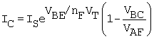
Figure B.8. Diodelike characteristics of the base currents. They are separately associated separately with their respective pn junctions. These currents do not couple across the base.

The equation has also been generalized to include the SPICE parameter nF, the forward current emission coefficient (which is usually assumed to be 1).
The base current, for the forward-biased base – emitter junction, is made up of two terms; these are the ideal base current (because it has the same VBE dependence as IC) and the leakage base current. The leakage component is typically small enough to be neglected and often is, for simplicity, in practice.
In the absence of leakage base current, the base current is
Equation B.8
![]()
where ISBE is the base – emitter saturation current. In the active mode, VBE is positive, and typically, VBE ≈ 0.6V. The exponential term is, for this case, exp(VBE/nFVT) ≈ 1010 such that the –1 is quite negligible. The –1 is necessary for the current to go to zero for VBE = 0. This current is due to (npn) injection and recombination of minority-carrier electrons in the base and injection and recombination of minority-carrier holes in the emitter. Base current could also be connected to injection of holes into the n-type emitter, which recombine at the emitter-contact metal – semiconductor interface. In any event, base – emitter junction base current is predominantly from injection into the emitter, as opposed to injection into the base.
For this case of no leakage current and for VBC = 0, the forward-active current gain (or current ratio) is defined as βDC ≡ βF. Using (B.6), (B.7), and (B.8) (with –1 neglected), this is
Equation B.9

and ISBE = IS/βF. Consequently, the ideal base current is normally written as
Equation B.10
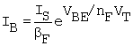
Note that the base current does not have VBC dependence as exhibited by the collector current. This is demonstrated to be valid in Project B.
The parameter βF is the SPICE transistor-model β. Implicit in the assignment of IS (IS) and BF (βF) in the SPICE device model is the assignment of the ideal base-current saturation ISBE = IS/βF. That is, there is no ISBE (SPICE parameter) in the model. If the general active-region relation for IC, (B.7), is now used in the βDC definition, we obtain the βDC relation for nonzero VBC, namely,
Equation B.11
![]()
where βF is a constant (SPICE BF) and βDC = βF for VBC = 0.
In the real transistor, there is, in general, a component of leakage current. It is associated with recombination of holes and electrons in the depletion region of the base – emitter junction. In SPICE, the leakage-current component is characterized with parameters nE (base – emitter leakage coefficient) and ISE (base – emitter leakage saturation current). When added to the ideal component, the total base current is
Equation B.12
(These are both positive into the transistor for the npn.) The parameter nE is ideally 2 (according to early, simplified theories), but in practice is typically about 1.5. When transistors are operated in or above the midrange of their rated current capacity, the leakage component becomes negligible.
For a small power transistor, the midrange starts at about 100 mA, such that the leakage term would be very significant at, for example, 1 mA. In the project on the transistor, which is designed to determine the SPICE parameters discussed here, a low-current range of less than about 1 mA is selected. The low current also avoids inadvertent rise in the temperature of the device during evaluation.
Similar equations that apply to the reverse-active mode can be obtained by direct substitution of the equivalent variables. The output current and input voltage, are, respectively, IE and VBC, while, for the reverse-active mode, VBE = 0 or negative. Based on the equivalent substitution
Equation B.13

The minus sign comes from having assigned the current direction of the emitter current out of the transistor (Fig. B.7). The parameter IS is common to (B.7) and (B.13). Equations (B.7) and (B.13) are combined to obtain the general case of VBE and VBC both positive (forward bias) in a following unit.
The reverse-operation base current is [the reverse-operation equivalent of (B.12)]
Equation B.14
![]()
where βR is the dc current ratio (reverse-active mode) for the case of no leakage component of base current, and is given by βR = IE/IB. In practice, the reverse ideal current gain is 0.1 < βR < 10, and therefore, the reverse-operated transistor is not a useful configuration in, for example, analog amplifiers. However, the reverse-active mode equations are essential, as is shown below, for developing the general equations for the forward mode. The general form includes the possibility that the transistor will be out of the active mode.
Although VAR (reverse Early voltage), ISC (reverse leakage saturation current) and nc (base – collector leakage emission coefficient) are officially SPICE parameters, we will not be concerned with these as they would rarely be a factor in the study of analog circuits.