
14.6. Output Buffer Stage
It is evident from the gain result, (14.29), that the high gain depends on having a high resistance at the output; a relatively small load resistor can reduce the gain substantially. For example, suppose that the amplifier is to be used as a resistance feedback amplifier as shown in Fig. 14.6. The input is at the gate of M2, and the feedback resistor is connected back to the gate of M1. The load at the output is Rf + R2 || RO.
Figure 14.6. Opamp with feedback resistor Rf. The feedback circuit adds load Rf + R2 in parallel with external load, RO, at the output.

For a specific example, assume that RO >> Rf >> R2 such that the load is approximately Rf. With the additional load, the gain (14.30) becomes
Equation 14.31
![]()
which is the result of Rf being in parallel with the output resistance of the common-source stage. Suppose that Rf = 10 kΩ and ID3 = 100 μA. In this case the gain would drop to about 400 (from about 4400), which would be unacceptable, as proper operation of opamps assumes a very high gain.
This loading problem is substantially eliminated with the addition of a buffer stage to isolate the load from the output node of the common-source stage, as shown in the circuit of Fig. 14.7. The source-follower buffer stage is made up of M6 and M13. The current-source bias transistor M13 also uses the reference voltage provided by M10. The load on the common-source stage of M3 is now infinite. The feedback network is included in the circuit for comparing with the diagrammatic version of the circuit of Fig. 14.6.
Figure 14.7. Three-stage amplifier with the addition of the source-follower (buffer) stage.

The gain expression of the source follower requires that the body effect be taken into consideration, as the body of M6 will be at signal ground. [The body of M6 will be attached to the negative supply voltage (not shown).] From Unit 7 it was shown that the source-follower stage gain, with resistor bias [(7.12)] for this case is
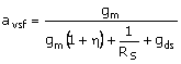
For the present case of current-source bias for the source-follower stage, the gain expression becomes, with inclusion now of the feedback network and the external load resistance of Fig. 14.7,
Equation 14.32
To obtain a quantitative sense of the body effect on the gain of the source follower, suppose that η = 0.15. Thus, in the limit for gm6 → ∞, avsf = 0.87. This is the best possible result, given the body effect.
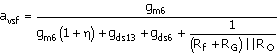
For a more general assessment, we can substitute the relations gm = 2ID/Veff, [(4.5)], and gds = IDλn [(14.15)] into (14.32) to obtain
Equation 14.33

We note that the terms associated with gds6 and gds13 are negligible. Minimization of the resistance term requires making gm6[(Rf + R2) || RO] >> 1 (making the output resistance of the source follower much less than the load resistance). This involves a combination of a large ID6 and kn6.
Suppose that ID6 = 400 μA, W6 = 500 μm, KPn = 100 μA/V2, and that the gate length is L = 10 μm. Recalling that kn = (KPn/2)(W/L) (Table 3.1), we obtain kn = 2500 μA/V2 and 1/gm6 = 500 Ω. Thus, for example, for RO = 10 kΩ, Rf = 10 kΩ, and Rf >> RG, avsf = 0.80, compared with the limiting value of avsf = 0.87. Thus the source follower functions very well to isolate the load from the high-gain common-source stage.
Finally, we write the overall gain expression, including a general load resistance, RL, by combining (14.29) and (14.32) as
Equation 14.34

A good approximation for the case of a sufficiently large gm6 is
Equation 14.35
![]()